Process for thick film circuit patterning

a technology of circuit patterning and thick film, which is applied in the direction of resistor manufacturing, liquid/solution decomposition chemical coating, metal pattern materials, etc., can solve the problems of thin film etch patterning approach for display and other applications, thin film photo-patterning method limitations, and narrow particle size distribution window

Inactive Publication Date: 2003-11-13
EI DU PONT DE NEMOURS & CO
View PDF20 Cites 19 Cited by
  • Summary
  • Abstract
  • Description
  • Claims
  • Application Information

AI Technical Summary

Problems solved by technology

The printed substrate is then dried which causes most of the solvent in the thick film composition to evaporate, and then fired which causes burnout of any organic vehicle.
Although screen print pattern resolution can be improved by optimizing screen wire-mesh dimensions, emulsion type, thickness, and screen printing variables; there is an accepted opinion in the industry that screen printed fine line and space resolution is not adequate for certain applications, since screen printed line resolutions are about 125 micron

Method used


Image

  • Process for thick film circuit patterning
  • Process for thick film circuit patterning
  • Process for thick film circuit patterning

Examples


example 1

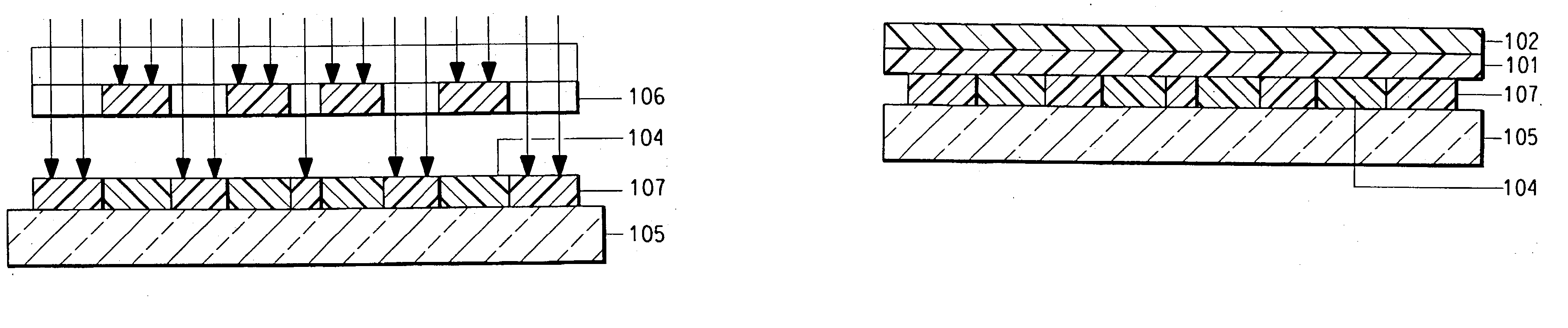
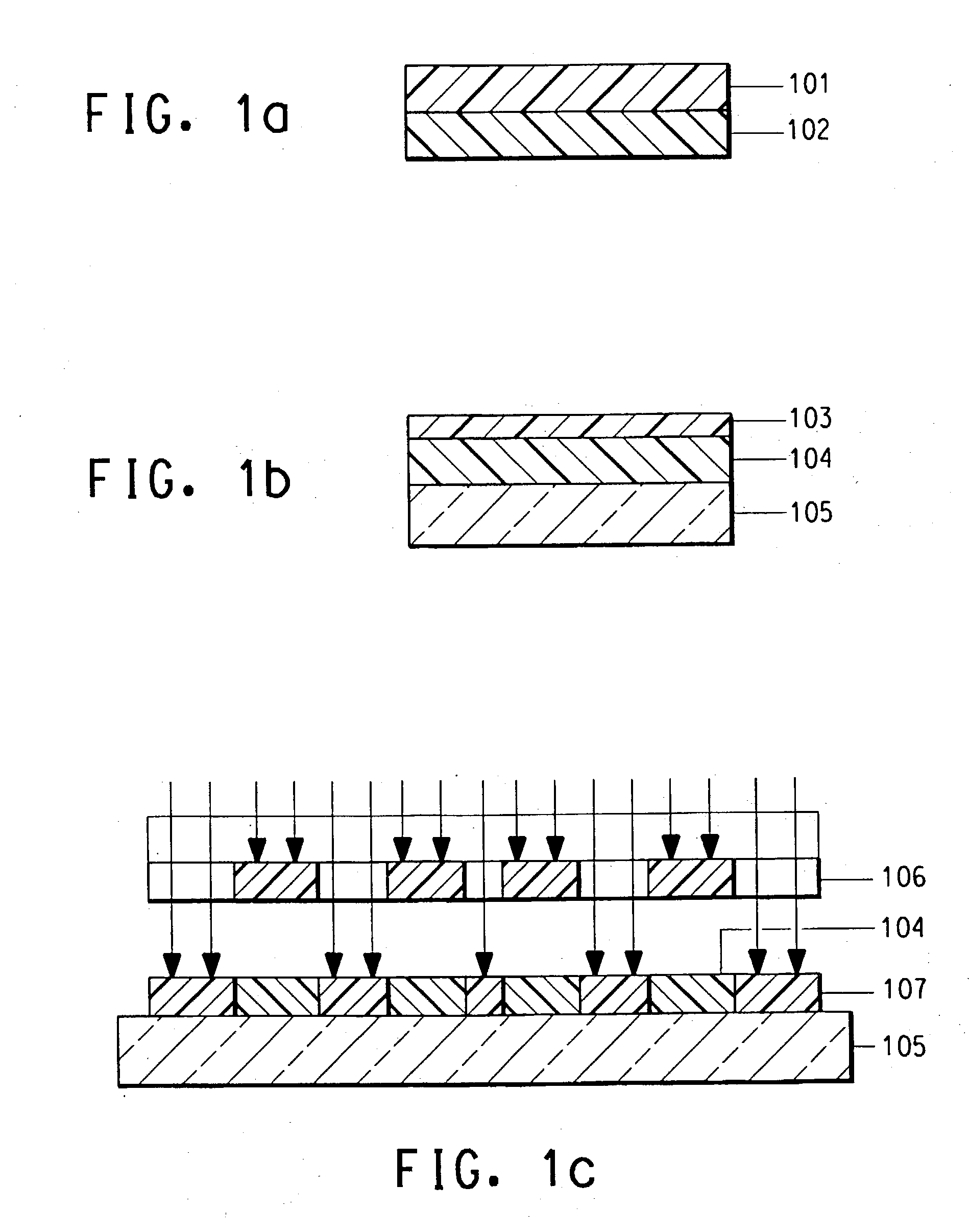
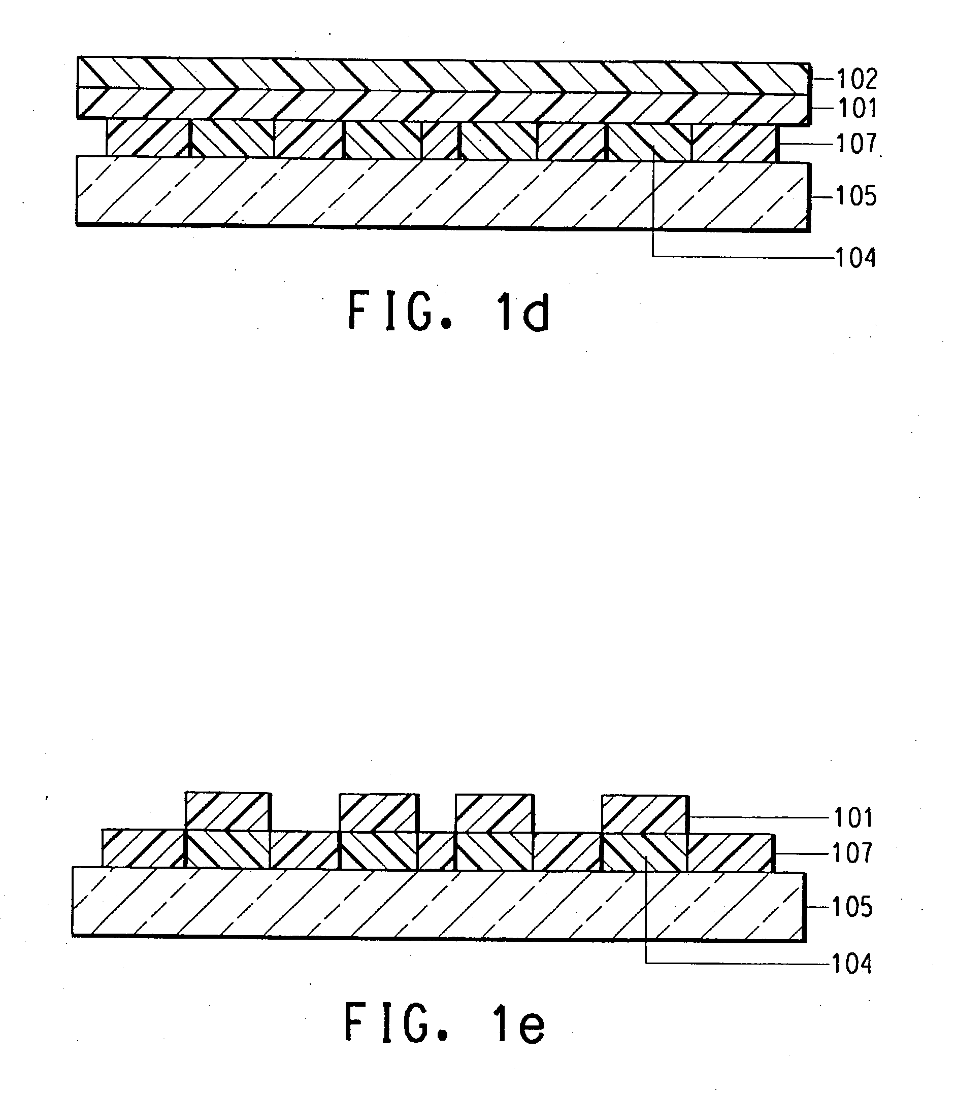
[0072] A positive CROMALIN.RTM. film, type ICFD (made by E. I. du Pont de Nemours and Company, Wilmington, Del.), having a coating weight in the range of 300 mg / dm.sup.2, was laminated (after peeling the removable base layer) to a soda lime glass substrate at about 250 d / F. The CROMALIN.RTM. film was exposed using a photomask circuit pattern (5KW UV bulb) for 15 units. The cover sheet on the imaged CROMALIN.RTM. film was peeled off. A transfer sheet was laminated onto the imaged film (with the thick film side of the transfer sheet facing the imaged layer). Peeling the transfer sheet produced the desired pattern where the unexposed areas of the imaged film layer remained tacky and the thick film was disposed on the tacky areas. The structure was fired at 500.degree. C. in air using a standard thick film firing profile for displays. The imaged film was completely burned out and the sintered, patterned thick film adhered strongly to the soda lime glass substrate. There was no detectabl...

example 2

[0073] The same process as Example 1 was repeated with the exception of no exposure of a CROMALIN.RTM. film and processed at a firing temperature of 585.degree. C. The CROMALIN.RTM. film (completely covered by the thick film composition of the transfer sheet) was burned out and adhesion of the thick film composition across the substrate surface was obtained.

example 3

[0074] The same process as Example 2 was repeated 6 times (imaged film / thick film composition / imaged film / thick film composition, etc.) and the six-layer imaged film / thick film composition was cofired at 585.degree. C. Similarly, all six layers of the imaged film were burned out and a thick film layer adhered to the glass substrate.


PUM

PropertyMeasurementUnit
Angleaaaaaaaaaa
Timeaaaaaaaaaa
Temperatureaaaaaaaaaa

Abstract

A process for patterning thick film electrically functional patterns using a photosensitive polymer layer. A tacky photosensitive layer is applied onto a substrate surface. The photosensitive layer is imaged with a pattern using actinic radiation, the exposed areas of the photosensitive layer become hardened and non-tacky. A subsequent application of a thick film composition sheet will cause the thick film to adhere to the remaining tacky areas. Upon peeling the sheet, a thick film print pattern will be produced. This step is followed by a processing profile prescribed by the thick film composition used which results in a pattern having electrically functional properties. The invention also extends to a process wherein a thick film composition is recovered from a used sheet.

Description

[0001] The invention relates to forming an electrically functional pattern on a substrate. More specifically, the invention relates to a process for using a photosensitive element in combination with a sheet having a thick film composition applied to a support. The invention also relates to a process for recovering the thick film composition from a used sheet.BACKGROUND OF INVENTION[0002] Established patterning methods used in the thick film industry include printing (screen or other), spraying, brushing, spin coating, dipping, laminating, photo-patterning and etching. Screen-printing is by far the most commonly used method for patterning thick film circuits. A certain amount of a thick film composition is placed at the edge of a printing screen wherein a squeegee moves and presses the thick film composition across the screen. A circuit pattern similar to the screen openings is printed on the substrate. The printed substrate is then dried which causes most of the solvent in the thic...

Claims


Application Information

Patent Timeline
IPC IPC(8): G03F7/004G03F7/34H05K1/09H05K3/04H05K3/20
CPCG03F7/0047G03F7/343H05K1/092H05K1/095Y10T428/2486H05K3/207H05K2203/0525Y10T428/24802H05K3/046Y10T428/31504
Inventor KEUSSEYAN, ROUPEN LEON
Owner EI DU PONT DE NEMOURS & CO
Why Eureka
Try Eureka