Ultra small size vertical MOSFET device and method for the manufacture thereof

a vertical mosfet, ultra-small technology, applied in the direction of semiconductor devices, electrical devices, nanotechnology, etc., can solve the problems of manufacturing nano-scale silicon devices in large quantities, and manufacturing nano-scale devices

Inactive Publication Date: 2004-01-15
ELECTRONICS & TELECOMM RES INST
View PDF0 Cites 22 Cited by
  • Summary
  • Abstract
  • Description
  • Claims
  • Application Information

AI Technical Summary

Benefits of technology

0008] It is, therefore, an object of the present invention to provide an ultra small size vertical MOSFET (metal oxide semiconductor field effect transistor) device having a vertical channel and a source / drain structure by applying a diffusion process without additional lithography steps.

Problems solved by technology

However, it has lot of obstacles to manufacture a nano-scale silicon device with a high performance by using a conventional manufacturing method.
But it is impossible to manufacture the nano-scale silicon device in large quantities because the e-beam direct writing method and x-ray lithography method are not definite techniques up to now.
Furthermore, since it is not only difficult to fabricate the nano-scale device with shallow source / drain junction depth using a single crystal silicon material but an electrical isolation property may also be deteriorated, there are difficulties in fabricating the device with the low voltage drivability.
Thus, in order to overcome the above problems, very complicated manufacturing processes are required.
However, this method has drawbacks that a structure of the MOS transistor is too complicated and further, a plurality of lithography, deposition and etch processes are required.
Additionally, it is hard to downsize the device because it is difficult to secure a process margin.
However, the MOS transistor having the vertical silicon channel in accordance with this conventional method has disadvantages as follows: first, it is difficult to secure a process margin owing to a complicated structure of the device; second, it is hard to fabricate the device in the trench of a micro size; third, it is difficult to grow up a single crystal silicon epi layer on a poly-crystal silicon; fourth, it is difficult to form a p-n junction on the channel of the single crystal and a diffusion layer of the poly-crystal; fifth, since source / drain contacts are formed on the channel of the single crystal and a diffusion layer of the poly-crystal, the junction leakage of source / drain contacts increases, besides a reliability and an insulating property of a gate insulating layer may be deteriorated.
According to this method, in order to fabricate the MOS transistor having the vertical silicon channel, complicated manufacturing steps should be carried out.
Therefore, it has problems that the manufacturing processes are too complicated and further, it is difficult to interconnect among the unit devices.
Although the e-beam direct writing method or x-ray lithography method is used, it is difficult to manufacture the device of nano-meter size in large quantities.
In addition, the conventional method using the silicon single crystal has large problems for forming shallow source / drain junction, ensuring a reliability of the nanometer scale device and isolation of each device electrically.

Method used


Image

  • Ultra small size vertical MOSFET device and method for the manufacture thereof
  • Ultra small size vertical MOSFET device and method for the manufacture thereof
  • Ultra small size vertical MOSFET device and method for the manufacture thereof

Examples


Embodiment Construction

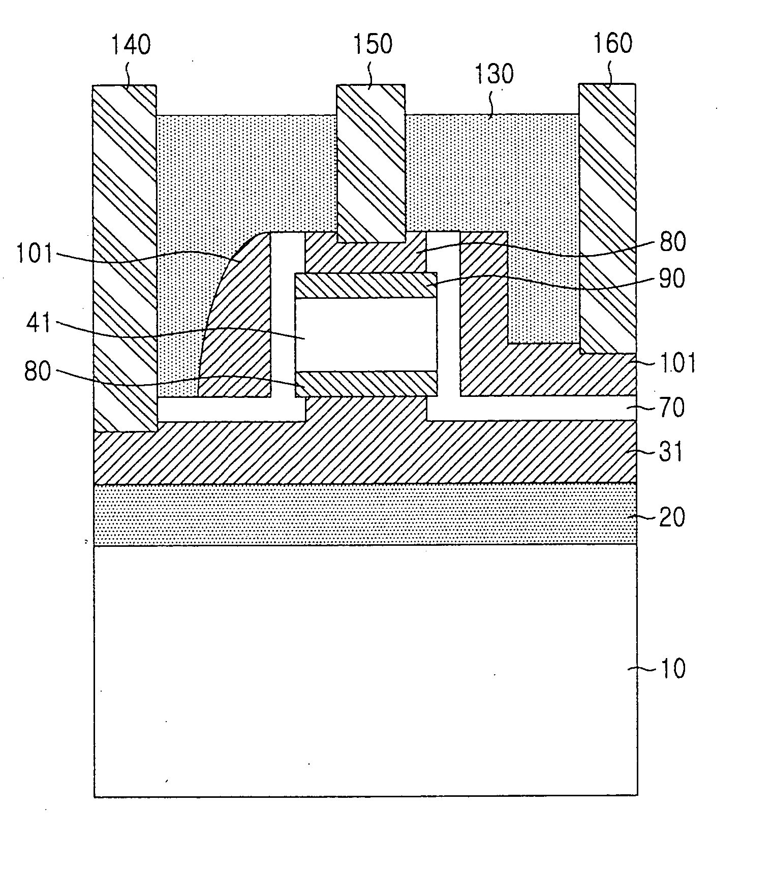
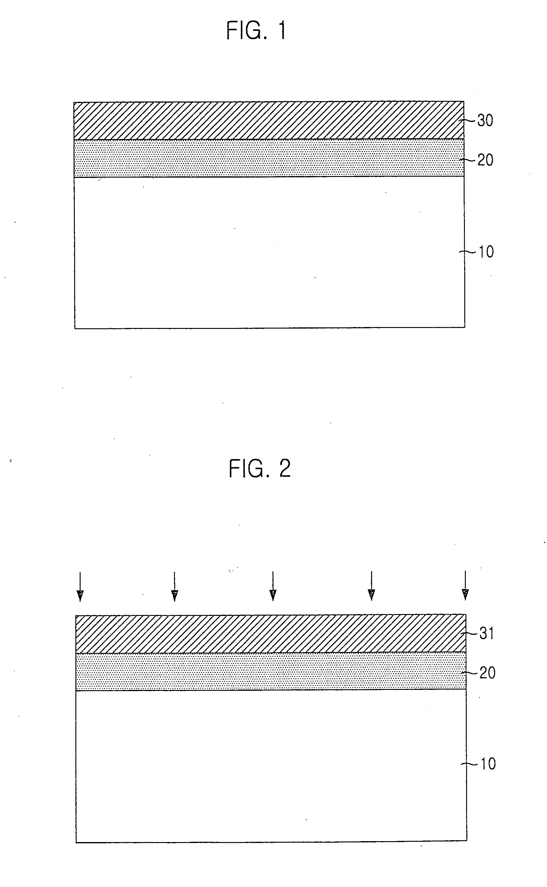
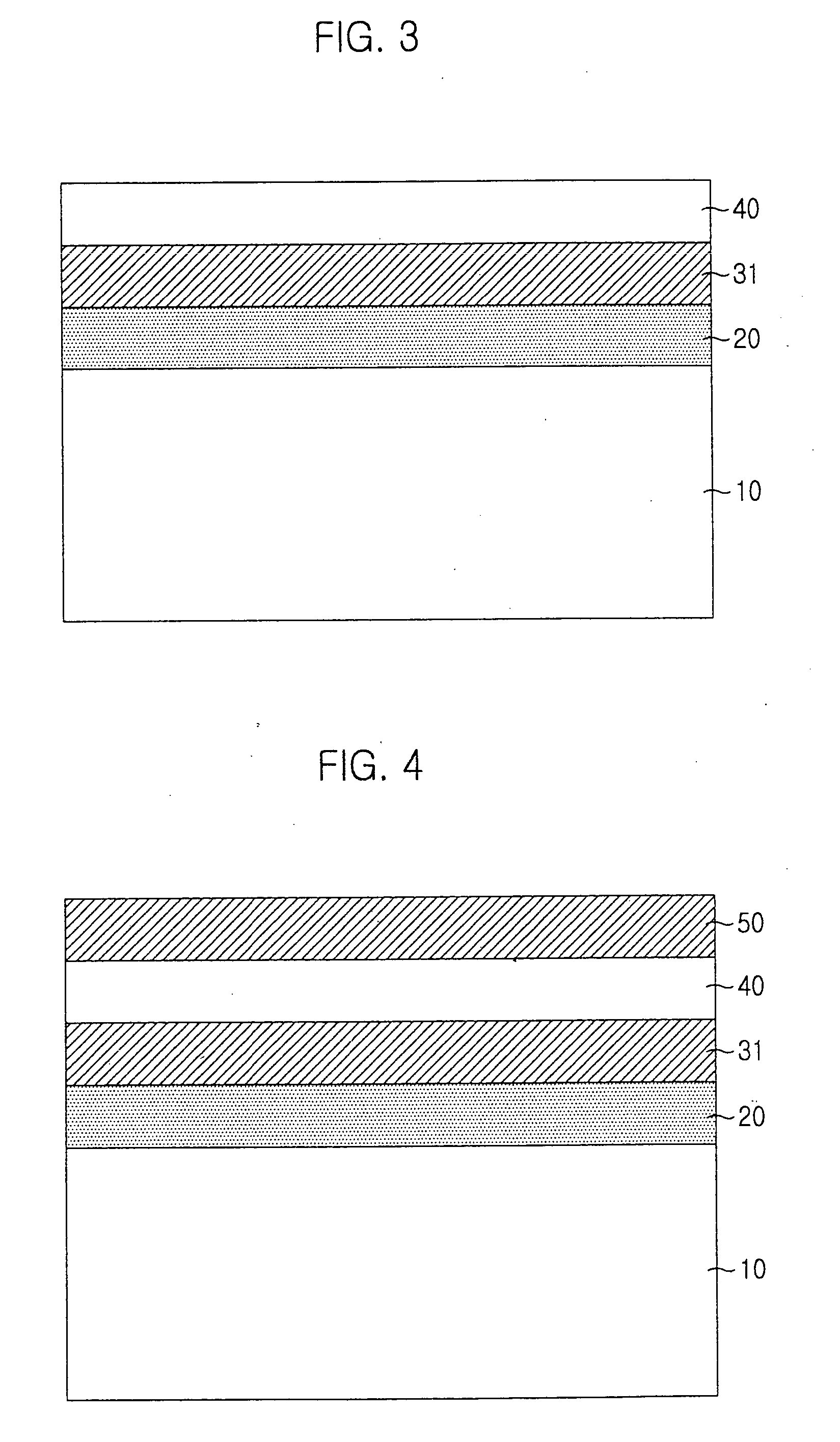
[0014] There are provided in FIGS. 1 to 11 cross sectional views setting forth an ultra small size vertical MOSET (metal oxide semiconductor field effect transistor) device and a method for the manufacture thereof in accordance with a preferred embodiment of the present invention. It is noted that the same reference numerals are used throughout multiple figures to designate the same components.

[0015] In FIG. 11, there is provided a cross sectional view of the inventive ultra small size vertical MOSFET device comprising an SOI (silicon on insulator) substrate, a channel 41, a source contact 80, a drain contact 90, a second silicon conductive layer 50, a gate insulating layer 70, a gate electrode 101, an interlayer dielectric (ILD) layer 130, a source interconnection 140, a drain interconnection 150 and a gate electrode interconnection 160. The SOI substrate includes a single crystal substrate 10, an oxide layer 20 formed upon the single crystal substrate 10 and a first silicon conduc...


PUM

PropertyMeasurementUnit
temperatureaaaaaaaaaa
concentrationaaaaaaaaaa

Abstract

The present invention relates to an ultra small size vertical MOSFET device having a vertical channel and a source/drain structure and a method for the manufacture thereof by using a silicon on insulator (SOI) substrate. To begin with, a first silicon conductive layer is formed by doping an impurity of a high concentration into a first single crystal silicon layer. Thereafter, a second single crystal silicon layer with the impurity of a low concentration and a second silicon conductive layer with the impurity of the high concentration are formed on the first silicon conductive layer. The second single crystal silicon layer and the second silicon conductive layer are vertically patterned into a predetermined configuration. Subsequently, a gate insulating layer is formed on entire surface. Then, an annealing process is carried out to diffuse the impurities in the first silicon conductive layer and the second silicon conductive layer into the second single crystal layer, thereby forming a source contact, a drain contact and a vertical channel. Finally, a gate electrode is formed on side walls of the vertical channel.

Description

FIELD OF THE INVENTION[0001] The present invention relates to a MOSFET (metal oxide semiconductor field effect transistor) device; and, more particularly, to an ultra small size vertical MOSFET device having a vertical channel and a source / drain structure and a method for the manufacture thereof by using a silicon on insulator (SOI) substrate.DESCRIPTION OF THE PRIOR ART[0002] In a silicon device technology, it is necessary to reduce a length of a channel, a depth of metallurgical junction at source and drain contact and a thickness of an effective gate insulating layer for achieving the silicon device with a low voltage, a high integration and a high speed drivability. Additionally, it is required the device with a high performance characteristic by an increase of a driving current and a decrease of a leakage current among the same size of the devices.[0003] However, it has lot of obstacles to manufacture a nano-scale silicon device with a high performance by using a conventional m...

Claims


Application Information

Patent Timeline
Patent Type & Authority Applications(United States)
IPC IPC(8): H01L27/12H01L29/78H01L29/786
CPCH01L27/1203H01L29/78642Y10S977/721Y10S977/712Y10S977/723Y10S977/887H01L29/78
Inventor CHO, WONJULEE, SEONG JAEPARK, KYOUNG WAN
Owner ELECTRONICS & TELECOMM RES INST
Why Eureka
Try Eureka