Conductive film, production method therefor, substrate provided with it and photo-electric conversion device

a technology of photoelectric conversion device and conductive film, which is applied in the direction of conductive layers on insulating supports, instruments, transportation and packaging, etc., can solve the problem of drop in the conversion efficiency of solar cells in an initial period of light irradiation

Inactive Publication Date: 2004-02-26
FUJISAWA AKIRA +3
View PDF2 Cites 56 Cited by
  • Summary
  • Abstract
  • Description
  • Claims
  • Application Information

AI Technical Summary

Problems solved by technology

However, optical deterioration is a problem with amorphous silicon because the irradiation of light generates defects, resulting in a drop in the conversion efficiency of the solar cell in an initial period of light irradiating.

Method used


Image

  • Conductive film, production method therefor, substrate provided with it and photo-electric conversion device
  • Conductive film, production method therefor, substrate provided with it and photo-electric conversion device
  • Conductive film, production method therefor, substrate provided with it and photo-electric conversion device

Examples


working examples

[0045] Hereinafter, Working Examples are used to describe the invention described in detail. However, the invention is not limited to the following examples.

working examples 1 to 3

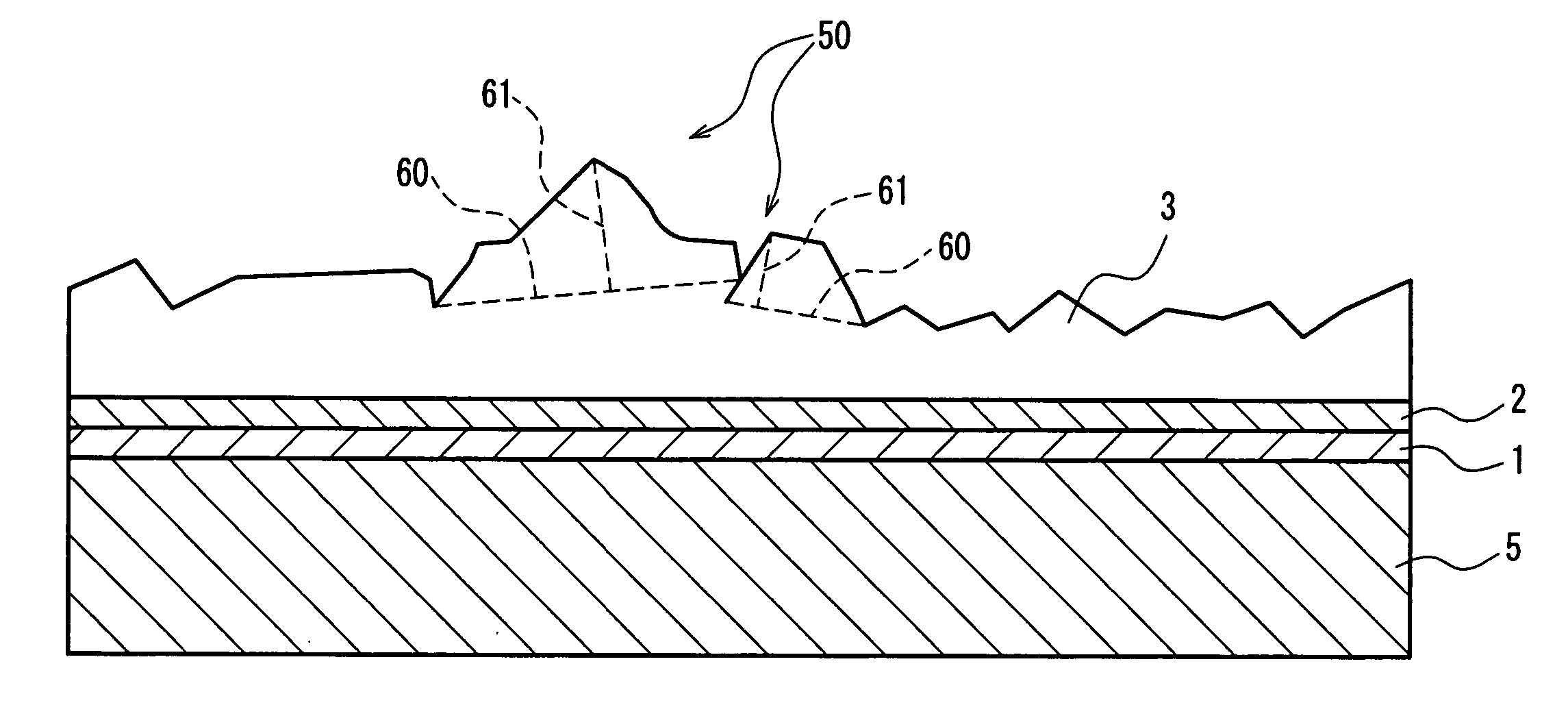
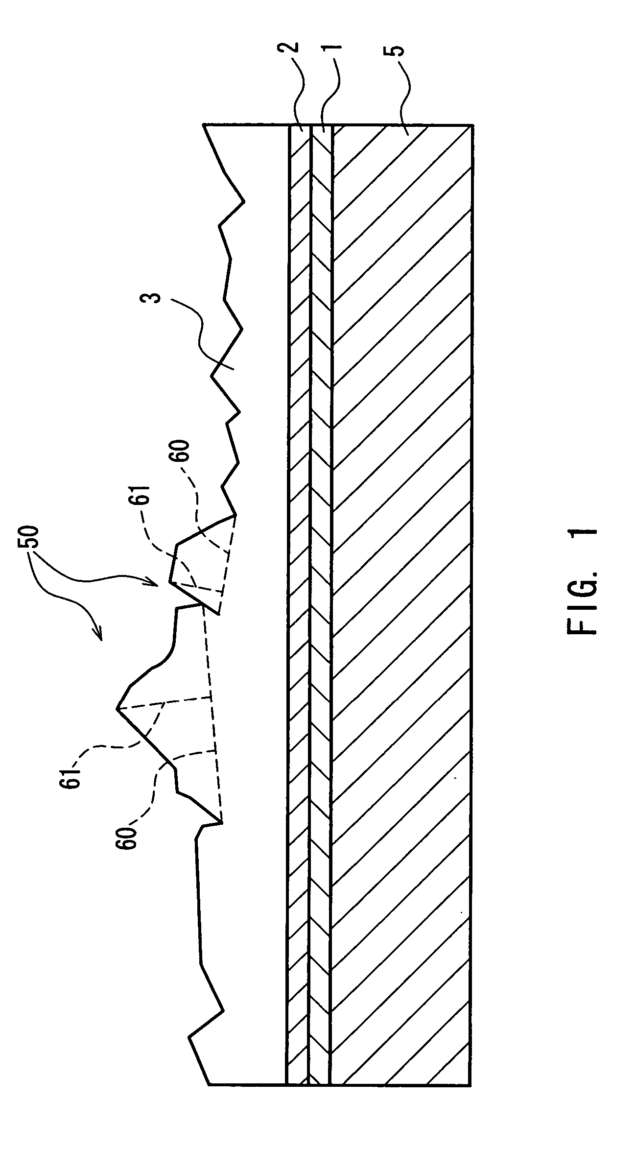
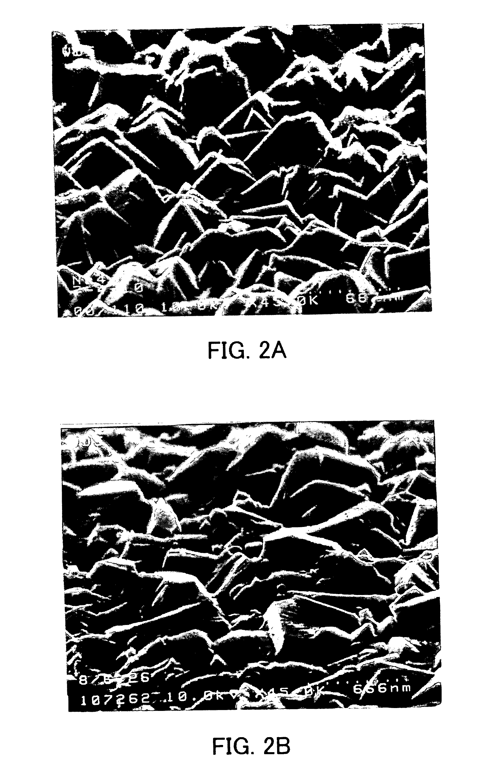
[0046] A 4 mm thick soda-lime glass sheet cut to 450.times.450 mm was placed on the mesh belt and sent through the heating furnace, heating it up to approximately 600.degree. C. As the heated glass sheet was delivered, coaters arranged above the delivery route supplied a mixture gas A constituted by monosilane, oxygen, and nitrogen, forming a silicon oxide thin film (undercoating film) with a film thickness of 25 nm on the glass sheet. After cooling the glass sheet, it was once again placed on the mesh belt and sent through the heating furnace, heating it up to approximately 600.degree. C. As the heated glass sheet was delivered, coaters arranged above the delivery route supplied a mixture gas B constituted by monobutyltin trichloride (vapor), oxygen, water vapor, nitrogen, and trifluoroacetate, forming a transparent conductive film made of fluorine-containing tin oxide (SnO.sub.2:F) on the silicon oxide thin film. The composition ratio of the components in the mixture gas B was 0.5...

working examples 4 and 5

[0049] Samples of photoelectric conversion elements were produced in the same manner as in Working Example 1 except that the composition ratio of the components in the mixture gas B was altered to 0.9 mol % of tin tetrachloride (vapor), 35 mol % to 37 mol % of water vapor, 62 mol % to 64 mol % of nitrogen, and 0.06 mol % of hydrogen fluoride, and the film thickness was changed to 810 to 840 nm. With respect to these samples, in the same manner as in Working Example 1, the height and the percentage occupied by the projections of the conductive film surface were calculated, the haze ratio was measured, and the photoelectric conversion efficiency and whether there was interface peeling was evaluated. The results are shown together in Table 1 below.


PUM

PropertyMeasurementUnit
thicknessaaaaaaaaaa
thicknessaaaaaaaaaa
haze ratioaaaaaaaaaa

Abstract

A conductive film which is formed on a substrate, wherein a total of areas of the base surfaces of protrusions at least 250 nm in height is at least 5% of the area of a surface on which this conductive film is formed. The conductive film mainly contains at least one kind of compound out of tin oxide, titanium oxide, indium oxide and zinc oxide, and is formed on a transparent substrate by a chemical vapor deposition using an oxygen atom-containing material as vapor. A photoelectric conversion device is formed by a conductive film-carrying substrate and at least one photoelectric conversion layer disposed on the substrate and containing a crystalline silicon thin film 1-5 mum in thickness.

Description

[0001] The present invention relates to conductive films used in photoelectric conversion elements and the like, and also relates to methods for manufacturing those conductive films, substrates provided with those conductive films, and photoelectric conversion devices using those substrates.[0002] Recent energy and environmental issues have led to an increased interest in solar cells. From the standpoint of conserving resources, thin-film type solar cells are likely to become mainstream. The following is a general configuration of a thin-film type solar cell. A transparent conductive film made of tin oxide (SnO.sub.2), for example, a photoelectric conversion layer made of an amorphous semiconductor such as amorphous silicon or amorphous silicon germanium, and a rear surface electrode are layered, in that order, on a transparent substrate such as a glass sheet.[0003] For solar cells, there is a demand for increased photoelectric conversion efficiency, and various technologies have be...

Claims


Application Information

Patent Timeline
Patent Type & Authority Applications(United States)
IPC IPC(8): C23C16/30C03C17/245C03C17/34C23C16/40C23C16/54H01B5/14H01B13/00H01L31/0236H01L31/04H01L31/18
CPCC03C17/245Y10T428/265C03C2217/211C03C2217/212C03C2217/215C03C2217/216C03C2218/152C23C16/40C23C16/407C23C16/545H01L31/0236H01L31/1884Y02E10/50Y10T428/24479C03C17/3482
Inventor FUJISAWA, AKIRANARA, MASATOSHISUEYOSHI, YUKIOHIRATA, MASAHIRO
Owner FUJISAWA AKIRA
Why Eureka
Try Eureka