Method and device for producing a coupling grating for a waveguide

a coupling grating and waveguide technology, applied in the direction of optics, instruments, light guides, etc., can solve the problems of inability to use industrially, inability to reproduce the production period of gratings of 500 nm even in laboratory conditions, and inability to produce gratings in laboratory conditions, etc., to reduce the contrast of fresnel diffraction images, reduce the disturbing diffraction effect, and reduce the effect of contras

Inactive Publication Date: 2004-03-04
GOMBERT ANDREAS +2
View PDF4 Cites 44 Cited by
  • Summary
  • Abstract
  • Description
  • Claims
  • Application Information

AI Technical Summary

Benefits of technology

0039] In an advantageous preferred embodiment, the device comprises in addition a special holding means for the exposure mask having a drive with which the mask can be moved perpendicular to the substrate surface along a defined path during exposure while maintaining the minimum distance. This embodiment of the device relates to a particular embodiment variant of the present method in which the distance between the exposure mask and the surface of the light-sensitive layer is altered during the exposure time. This alteration, which can be realized for example by a simple lin

Problems solved by technology

However, this prior art contact method of exposure has the disadvantage that it cannot be used industrially for grating periods of <2 .mu.m, because the production rejects due to unavoidable variations in the distance between mask and the substrate with small grating periods would be too high.
With this method, the production of grating periods of <500 nm is not reproducible even in laboratory conditions.
Another drawback of this contact exposure method is that the writing time of the electron-beam writer for the exposure mask is approximately 1h/mm.sup.2, thus very high.
The production of an exposure mask for grating structures with periods of <1000 nm on areas of more than 50 mm.sup.2 would require writing times of approximately 50 hours so that the costs, in particular for small-scale production, would be unacceptable.
However, this requires a projection exposure machine with exposure wavelengths in the low UV range.
Such exposure machines are so expensive that their depreciation makes up a major part of the structuring costs.
Consequently, this method is presently not implemented in industry.
Another disadvantage of this method is that projection exposure requires extremely plane substrates due to the low dept

Method used


Image

  • Method and device for producing a coupling grating for a waveguide
  • Method and device for producing a coupling grating for a waveguide
  • Method and device for producing a coupling grating for a waveguide

Examples


Embodiment Construction

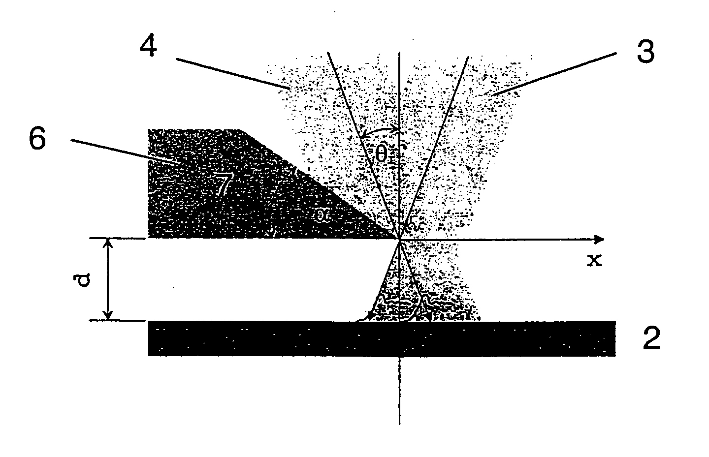
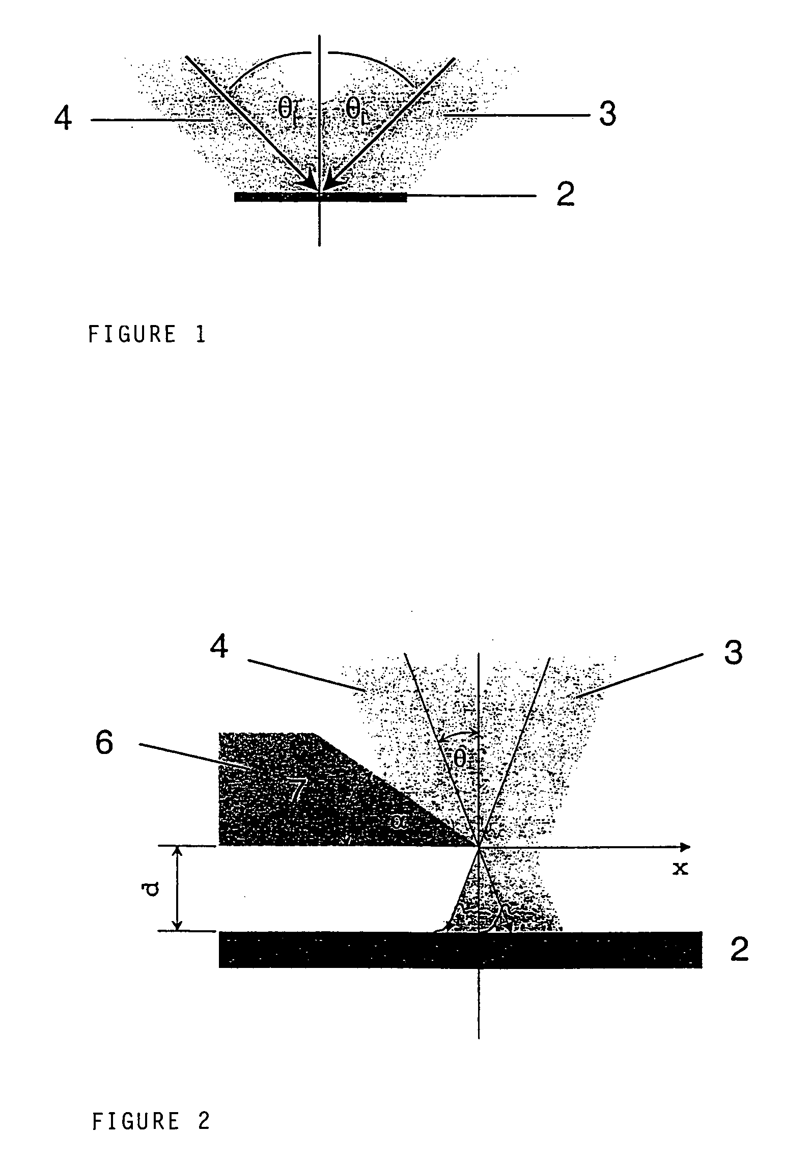
[0047] FIG. 1 shows a schematic representation of an example of the exposure of the surface of a light-sensitive layer 2 with two coherent light beams 3,4. Both the light beams are superimposed at a fixed angle of .theta..sub.i on the surface of the light-sensitive layer 2. This representation shows neither the substrate on which the light-sensitive layer is applied nor the exposure mask to set the boundaries of the to-be-produced coupling grating. The wavelength .lambda..sub.0 of the two irradiated light beams and the incident angle .theta..sub.i yield a fixed spatial intensity modulation having a period of .LAMBDA. which corresponds to the to-be-produced grating period.

[0048] In the present example, a coupling grating matrix having a grating period of .LAMBDA.=500 nm should be produced. For this purpose, an argon ion laser having an emission wave length of 364 nm is employed. The output beam of this laser is split into two partial beams, which are widened using corresponding optic...


PUM


Abstract

The invention relates to a method and a device for producing a coupling grating (5) for a waveguide. The method relies on the technique of interference lithography, whereby an interference pattern on a light-sensitive layer (2) is exposed by superimposing two coherent light beams (3, 4) on said light-sensitive layer (2). Said pattern is then transferred onto the surface of the substrate (1) that lies underneath by subsequent developing and an etching process. The method is characterized in that it uses a shadow mask (6) that is mounted at minimum clearance relative to the surface of the light-sensitive layer (2). By observing said minimum clearance, the Fresnel diffraction images of both light beams (3, 4) are separated on the edge(7). The thickness of the light-sensitive layer (2) is selected in such a way that the superimposition of the Fresnel diffraction pattern of one light beam with the other undisturbed light beam suffices to uncover areas of the substrate (1) during subsequent developing of the layer (2). The method makes it possible to avoid transfer of unwanted diffraction effects on the edge of the shadow mask to the substrate. The method provides a cost-effective solution for the production of large-surface coupling grating matrices.

Description

FIELD OF APPLICATION[0001] The present invention relates to a method for producing a coupling grating for a wavequide utilizing interference lithography, in which a light-sensitive layer on a substrate is exposed with an interference pattern produced by superimposing two coherent light beams and subsequently developed. The areas of the substrate that development laid bare undergo an etching process after which the light-sensitive layer is removed from the substrate. Furthermore, the invention relates to a device for carrying out the method.[0002] Using coupling gratings to couple radiation into waveguides, particularly in integrated optical waveguides, is widespread. For example coupling gratings are produced on the surface of a glass substrate and the waveguide is applied to this structure as a highly diffracting layer. Typical grating periods for coupling gratings for coupling in visible light range from 300 to 1000 nm. The depth of the structure in the surface of the substrate, h...

Claims


Application Information

Patent Timeline
IPC IPC(8): G02B6/12G02B6/124G02B6/136
CPCG02B6/124G02B2006/12173G02B2006/12107G02B6/136
Inventor GOMBERT, ANDREASNIGGEMANN, MICHAELLERCHENMULLER, HANSJORG
Owner GOMBERT ANDREAS
Why Eureka
Try Eureka