Mold and method of producing the same

a technology of mold and dough, applied in the direction of dough shaping, manufacturing tools, instruments, etc., can solve the problems of long time-consuming and labor-intensive, complex devices, and difficult to realize devices for accomplishing active alignment maintaining the desired accuracy,

Inactive Publication Date: 2004-03-11
KOSUGA HIROYUKI +1
View PDF12 Cites 51 Cited by
  • Summary
  • Abstract
  • Description
  • Claims
  • Application Information

AI Technical Summary

Benefits of technology

[0018] A second object of the present invention is to provide a method of easily producing a mold for press-molding having a highly precise transfer molding surface constituted by a plurality of transfer patterns.
[0019] A third object of the present invention is to provide a mold which capable of easily obtaining the one for press-molding having transfer patterns of a predetermined shape maintaining a high accuracy and featuring an extended life of the transfer patterns, and a method of producing the mold.
[0020] A fourth object of the present invention is to provide a method of producing a diffraction element of a glass at a low cost.

Problems solved by technology

However, the optical interconnection based on the active alignment requires an extended period of time since the precision stage must be driven over a wide range as described above.
Moreover, the automated operation causes the structure of the device to become complex, which makes it difficult to realize a device for accomplishing the active alignment maintaining a desired accuracy.
Fabricating the mold relying upon the conventional method, however, involves difficulties as described below.
At the time of forming the surface that becomes the side surface of the mold, however, it is difficult to prevent the occurrence of pitching on this surface.
Occurrence of pitching makes it difficult to correctly specify the position of the surface.
After the chamfering, however, it becomes difficult to correctly specify the position of the above-mentioned surface (which becomes the side surface of the mold).
On account of these reasons, the conventional method in which a surface to be become the side surface of the mold is, first, formed on the mold material, and the transfer molding surface is formed by machining by using this surface as a reference surface, involves too many difficulties in obtaining a mold having highly precise transfer molding surfaces constituted by the plurality of transfer patterns.
However, these molds have a defect in that the transfer pattern itself has a shorter life than that of the mold in which the transfer pattern is formed on the mold material.
In the case of the machine work, however, the tip of a cutting tool does not enter into a portion where straight protruded portions intersect each other, making it difficult to accurately form the alignment mark transfer portion(s) or the shaping portion(s) having intersecting portion(s).
Moreover, when it is attempted to obtain the mold A having a step in the transfer molding surface (excluding the step between the alignment mark transfer portion and the surrounding thereof), it is not allowed to introduce the tip of the cutting tool for machine work near to the step in the region on the lower side divided by the step.
Therefore, limitation is imposed on the region where the alignment mark transfer portion(s) or the shaping portion(s) can be formed by machine work.
Furthermore, it is difficult to form, by wet etching, the highly precise alignment mark transfer portion(s) or the shaping portion(s) on the mold material composed of the above-mentioned hard material, cermet, SiC or amorphous carbon.
Moreover, the molds constituting the set of molds may or may not have a mold release film.

Method used


Image

  • Mold and method of producing the same
  • Mold and method of producing the same
  • Mold and method of producing the same

Examples


example 2

[0195] (1) Preparation of a First Mold by the Method aI.

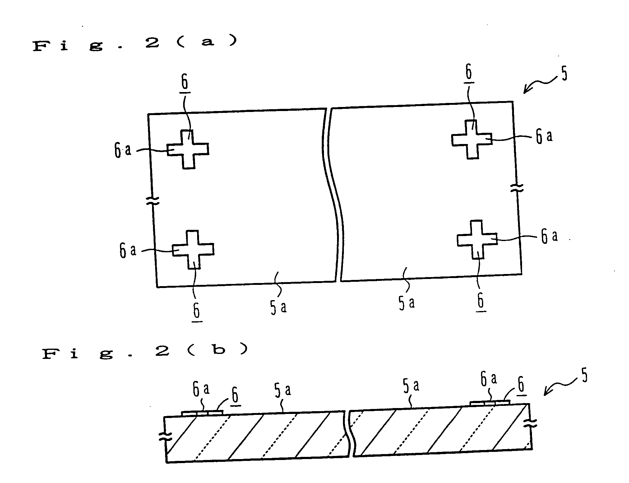
[0196] First, a hard material containing WC is used as a mold material. The mold material has the shape of a flat plate measuring 30.0 mm long, 20.0 mm wide, 1.0 mm thick and having a maximum surface roughness of 100 angstroms. Next, resist patterns of a crossed shape measuring 10 .mu.m long, 10 .mu.m wide, 2.0 .mu.thick and having a line width of 3.0 .mu.m as viewed on a plane are formed at four corners on one surface of the mold material quite in the same manner as in Example 1(1).

[0197] The resist patterns are post-baked at 120.degree. C. for 60 minutes. Then, by using these resist patterns as masks, one surface of the mold material is dry-etched for 10 minute. The dry-etching is effected by using a reactive etching apparatus of the type of Inductively Coupled Plasma, and an Ar gas and a CF, gas are used as etching gases. The etching conditions consist of a coil bias of 600 W, a substrate bias of 600 W, an Ar gas flow rate o...

example 3

[0212] (1) Preparation of a First Mold by the Method aII.

[0213] First, amorphous carbon is used as the mold material. The mold material has the shape of a flat plate measuring 20.0 mm long, 10.0 mm wide, 3.0 mm thick and having a maximum surface roughness of 200 angstroms. Next, a negative-type electron beam resist (ZEP7000 produced by Nippon Zeon Co.) is applied by a spin-coating method onto one surface of the mold material to form a resin layer maintaining a thickness of 1.5 .mu.m on one surface of the mold material.

[0214] Next, by using an electron beam (exposure of 55 .mu.C / cm.sup.2), equilateral triangles of a side of 50 .mu.m long (each side having a line width of 5.0 .mu.m) are drawn at four corners on the resin layer as viewed on a plane. The resin layer after drawn with the electron beam is developed by being immersed in a predetermined developing solution (ZEP500 produced by Nippon Zeon Co.) for 90 seconds.

[0215] The portion of the resin layer that is not drawn with the el...

example 4

[0230] (1) Preparation of a First Mold by the Method aI.

[0231] First, a hard material of the same composition as the hard material used in Example 1 is used as the mold material. The mold material has the shape of a flat plate measuring 20.0 mm long, 10.0 mm wide and 2.0 mm thick. One edge in the direction of length on one surface of the mold material is cut and removed into a predetermined width and a thickness to form a flat surface (hereinafter, the flat surface that is polished as described later is referred to as "flat surface for forming a first transfer portion"). Furthermore, both edges (excluding the flat surface for forming the first transfer portion) in the direction of width on the surface of the mold material are cut and removed over a predetermined width and thickness to form flat surfaces (a total of two flat surfaces; hereinafter these flat surfaces after polished are generally referred to as "flat surfaces for forming second transfer portions"), and these flat surfa...


PUM

PropertyMeasurementUnit
surface roughnessaaaaaaaaaa
thicknessaaaaaaaaaa
surface roughnessaaaaaaaaaa

Abstract

(1) Alignment mark transfer portion(s) is / are formed on the transfer molding surface of a mold that is used for press-molding a optical element fixing member and having alignment marks; (2) alignment mark(s) is / are formed on the mold material by dry-etching, and the mold material is worked using the alignment mark(s) as a reference to form the transfer molding surface constituted by a plurality of transfer patterns, in order to obtain a mold for press-molding; and (3) the transfer patterns are formed by dry-etching, or a transfer molding bare surface for transfer patterns is formed by dry-etching and a mold release film is formed thereon to reflect the shape of the transfer molding base surface, in order to obtain a mold for press-molding.

Description

[0001] The present invention relates to a mold for obtaining a desired molded article by press-molding, to a method of producing the mold, and to a molded article obtained by using the mold.DESCRIPTION OF THE PRIOR ART[0002] Press-molding is a technology which makes it possible to produce molded articles having a predetermined shape maintaining a high productivity once a mold used for the press-molding is fabricated. At present, therefore, the molded articles of a variety of shapes have been produced by press-molding. Moreover, the press-molding makes it possible to mass-produce the molded articles maintaining high accuracy. Nowadays, therefore, products that require high degree of accuracy, such as optical element fixing member and diffraction elements, have been produced by press-molding.[0003] Here, the "optical element fixing members" referred to as in this specification stand for members that are used for fixing or mounting a predetermined number of elements required for the tr...

Claims


Application Information

Patent Timeline
Patent Type & Authority Applications(United States)
IPC IPC(8): B29C33/38B29C33/42C03B11/08G02B6/36G02B6/42
CPCB29C33/3842B29C33/42C03B11/08C03B11/082C03B2215/412C03B2215/413C03B2215/404G02B6/3636G02B6/3652G02B6/3692G02B6/3696G02B6/4224C03B2215/414Y02P40/57
Inventor KOSUGA, HIROYUKIYOKOO, YOSHIATSU
Owner KOSUGA HIROYUKI
Why Eureka
Try Eureka