High reliability multlayer circuit substrates and methods for their formation

a multi-layer circuit and substrate technology, applied in the field of multi-layer wiring substrate formation, can solve the problems of limiting the usefulness of multi-layer substrate production, complex hybrid circuits typically require equally complex interconnection structures, and the use of refractory substrates in high-temperature processing

Inactive Publication Date: 2004-04-01
MEDTRONIC MIMIMED INC
View PDF8 Cites 341 Cited by
  • Summary
  • Abstract
  • Description
  • Claims
  • Application Information

AI Technical Summary

Problems solved by technology

Complex hybrid circuits typically require equally complex interconnection structure.
Various conventional lamination techniques are known, however each has limitations that restricts its usefulness for producing multilayer substrates.
As a result, substrates formed by high temperature processing are limited to the use of refractory metal conductors such as tungsten and molybdenum, which have very low resistance to corrosion in the presence of moisture and are therefore not appropriate for use in harsh environments.
However the dielectric materials used in low-temperature processes are generally provided with a high glass content and therefore have relatively poor resistance to environmental corrosion, as well as a relatively low dielectric constant and relatively poor thermal conductivity.
However, thick film techniques require the use of relatively thick dielectric layers and thus it is difficult to produce a thin multilayer substrate using thick film techniques.
Thick film dielectrics also have relatively low dielectric constants, relatively poor thermal conductivity, and poor corrosion resistance.
In addition to the problems listed above, the conventional lamination techniques cannot use green sheets of less than 0.006 inches in thickness because thinner green sheets cannot reliably survive necessary processing such as drilling or punching of via holes.
Also, because the

Method used


Image

  • High reliability multlayer circuit substrates and methods for their formation
  • High reliability multlayer circuit substrates and methods for their formation
  • High reliability multlayer circuit substrates and methods for their formation

Examples


Embodiment Construction

Minimum line width 0.005 inches 0.001 inches Minimum dielectric thickness 0.006 inches 0.00004 inches Minimum via diameter 0.005 inches 0.002 inches Minimum via spacing 0.015 inches 0.006 inches Shrinkage in excess of 10% none

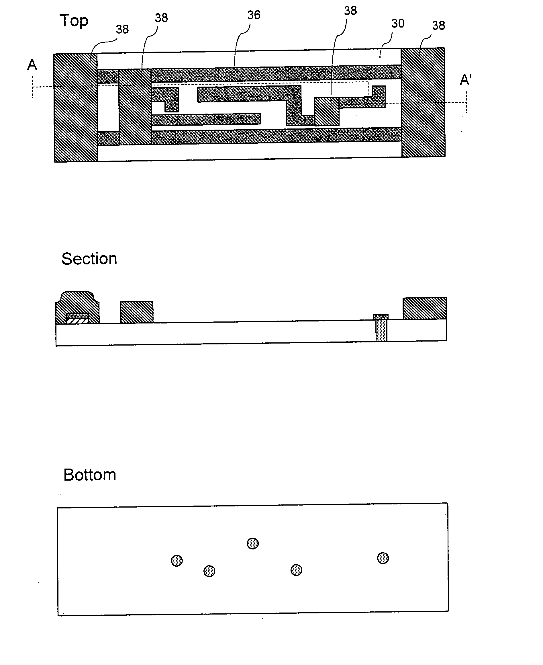
[0053] While the multilayer substrate of the preferred embodiment is comprised solely of vias, conductors and dielectric layers, alternative embodiments may integrate or embed passive components such as capacitors, resistors and inductors into the multilayer substrate. For example, while the circuit of the preferred embodiment comprises a discrete capacitor, in alternative embodiments a capacitor may be integrally formed in the multilayer substrate from conductors separated by a deposited dielectric layer. Capacitors may be formed, for example, using a silicon oxide or silicon nitride dielectric layer between conductive plates. Interdigitated capacitors and trench may also be formed. The degree of material control and geometrical precision provided by vacuum de...


PUM


Abstract

A multilayer circuit substrate for multi-chip modules or hybrid circuits includes a dielectric base substrate, conductors formed on the base substrate and a vacuum deposited dielectric thin film formed over the conductors and the base substrate. The vacuum deposited dielectric thin film is patterned using sacrificial structures formed by shadow mask techniques. Substrates formed in this manner enable significant increases in interconnect density and significant reduction of over-all substrate thickness.

Description

[0001] This application claims priority under 35 USC .sctn.119(e) from U.S. Provisional Application Serial No. 60 / 414,289, filed Sep. 27, 2002, entitled "Multilayer Substrate," the entirety of which is incorporated herein by reference.[0002] This application is a continuation-in-part claiming priority under 35 USC .sctn.120 from U.S. patent application Ser. No. 10 / 331,186, filed Dec. 26, 2002, entitled "Multilayer Substrate," the entirety of which is incorporated herein by reference.[0003] This application related to U.S. patent application Ser. No. 10 / 038,276, filed Dec. 31, 2001, entitled "Sensor Substrate and Method of Fabricating Same," the entirety of which is incorporated herein by reference.[0004] 1. Field of the Invention[0005] Embodiments of the invention relate to semiconductor device fabrication, and, in particular, to the formation of multilayer wiring substrates on which integrated circuits or discrete devices are mounted.[0006] 2. Description of Related Art[0007] A var...

Claims


Application Information

Patent Timeline
IPC IPC(8): H01L21/48H05K1/16H05K3/04H05K3/40H05K3/46
CPCH01L21/4857H01L2924/19107H05K1/162H05K3/048H05K3/4053H05K3/4061H05K3/4664H05K3/467H05K2201/0179H05K2203/0278H05K2203/085H05K2203/1476H05K2203/308H01L2924/0002H01L21/4867H01L2924/00
Inventor SHAH, RAJIVPENDO, SHAUN
Owner MEDTRONIC MIMIMED INC
Why Eureka
Try Eureka