Laser irradiation apparatus and method of manufacturing semiconductor device

a laser irradiation and semiconductor technology, applied in the direction of manufacturing tools, laser beam welding apparatus, welding apparatus, etc., can solve the problems of inferior heat resistance of glass substrate, easy shape change, and inability to uniformly irradiate laser light on the whole semiconductor film

Active Publication Date: 2004-04-08
SEMICON ENERGY LAB CO LTD
View PDF29 Cites 50 Cited by
  • Summary
  • Abstract
  • Description
  • Claims
  • Application Information

AI Technical Summary

Problems solved by technology

However, a glass substrate is inferior in heat resistance and easy to change its shape when heated.
Therefore, when the f.theta. lens is used as it is for crystallization by a laser,

Method used


Image

  • Laser irradiation apparatus and method of manufacturing semiconductor device
  • Laser irradiation apparatus and method of manufacturing semiconductor device
  • Laser irradiation apparatus and method of manufacturing semiconductor device

Examples


embodiment 1

[0050] [Embodiment 1]

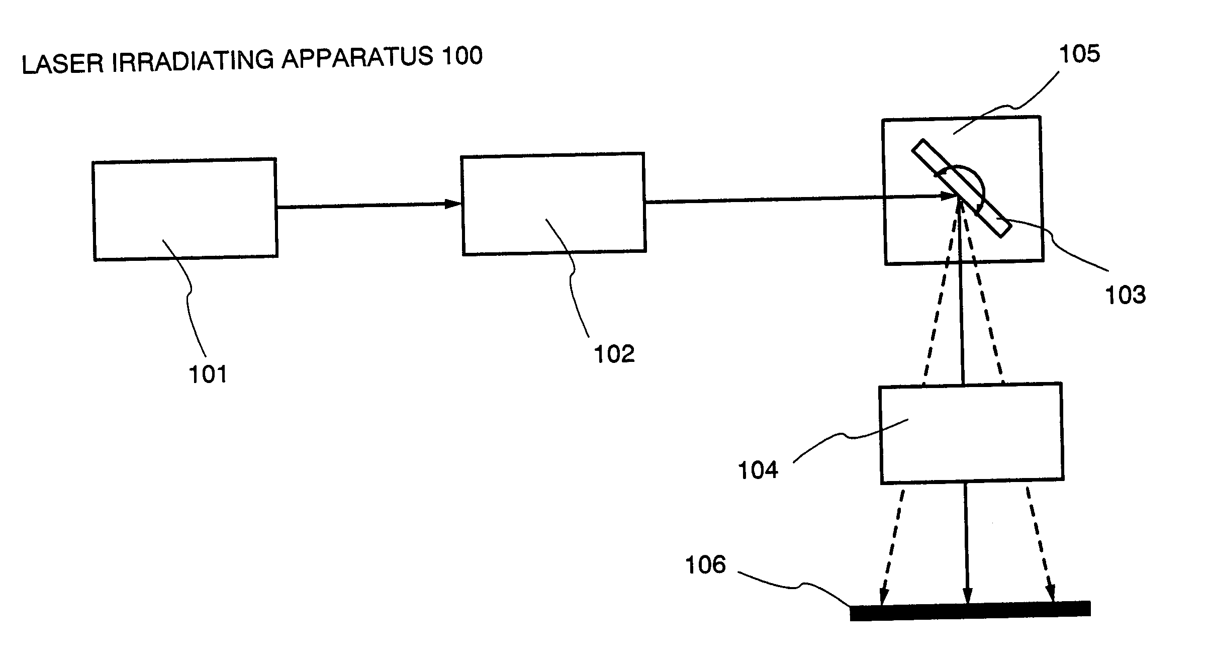
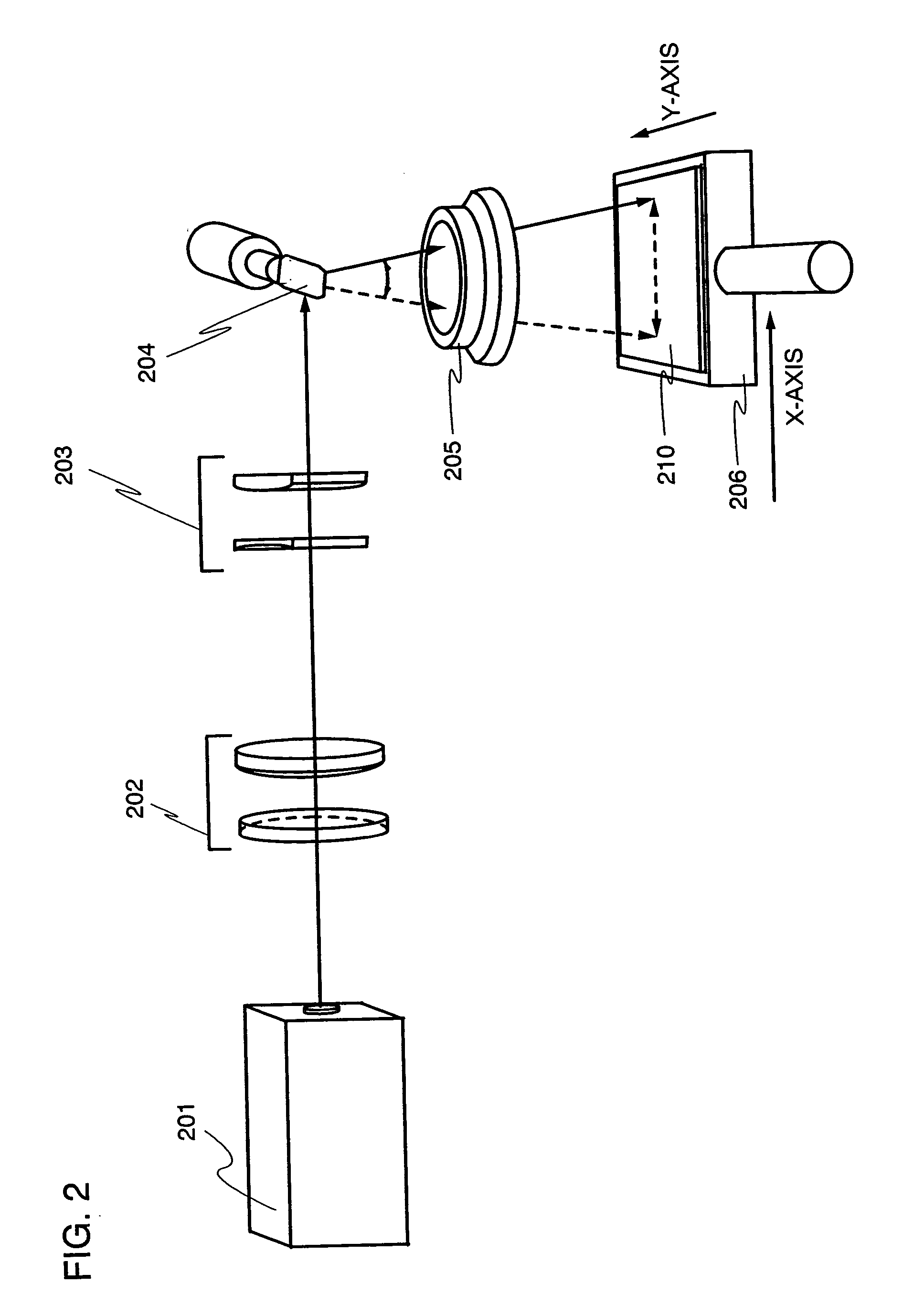
[0051] FIG. 2 shows an example of the laser irradiation apparatus according to the present invention. The laser beam emitted from the laser oscillator 201 is converted into a line shaped beam through a beam expander 202 and a cylindrical lens 203. A galvanometer mirror 204 and an f.theta. lens 205 are arranged over the substrate 210. The beam reflected by the galvanometer mirror 204 is incident into the f.theta. lens 205. The converted line shaped beam can be constantly focused on the substrate by the f.theta. lens 205. It is noted that a telecentric lens may be used as the f.theta. lens 205. The incident angle of the laser light to the substrate can be kept constant by the telecentric lens regardless of the place in the lens where the laser light is incident and thereby the reflectance of the object to be irradiated can be also kept constant. It is noted that in the case that the laser light is irradiated on the substrate like a glass substrate where the laser ...

embodiment 2

[0057] [Embodiment 2]

[0058] In this embodiment, the case that the scanning of the laser light in the embodiment 1 is performed by controlling the galvanometer mirror in both X-axis and Y-axis direction is explained.

[0059] The scanning speed of the laser light by the galvanometer mirror is explained. First, the operating speed of the galvanometer mirror is controlled so as to keep the scanning speed of the laser light on the substrate constant. Since the transmissivity depends on the place in the lens in this case, the energy of the laser light scanned also depends on the change of the transmissivity. FIG. 6 shows an example of the change in the irradiation energy of the laser light scanned on the substrate in this case. FIG. 6 indicates that the laser intensity is high in the vicinity of the center of the substrate and it becomes attenuated toward the edge of the substrate concentrically. Therefore, the change in the irradiation energy on the substrate can be suppressed by increasin...

embodiment 3

[0063] [Embodiment 3]

[0064] In this embodiment, a process up to manufacture a semiconductor device with the crystalline semiconductor film by using the laser irradiation apparatus of the present invention is described with FIG. 10 and FIG. 11.

[0065] First of all, base films 1001a and 1001b are formed on the substrate 1000. As the substrate 1000, an insulating substrate such as a glass substrate, a quartz substrate, or a crystalline glass substrate, or a ceramic substrate, a stainless substrate, a metal substrate (tantalum, tungsten, molybdenum, and the like), a semiconductor substrate, a plastic substrate (polyimide, acrylic, polyethylene terephthalate, polycarbonate, polyarylate, polyether sulfon and the like) can be used. It is noted that the substrate shall be made from the material that can resist the heat generated through the processes. A glass substrate is used in this embodiment.

[0066] As the base films 1001a and 1001b, a silicon oxide film, a silicon nitride film or a silic...


PUM

PropertyMeasurementUnit
Speedaaaaaaaaaa
Shapeaaaaaaaaaa
Energyaaaaaaaaaa

Abstract

The transmissivity of an ftheta lens which is used as a means for converging laser light differs in the center and in the edge thereof. As a result, when the ftheta lens is used as it is with the purpose of crystallizing by laser irradiation, energy distribution of the laser light which is irradiated on the semiconductor film is not uniform so that the whole surface of the semiconductor film could not be irradiated uniformly. Therefore, the present invention provides a laser irradiation apparatus including a galvanometer mirror and an ftheta lens that can offset the change of the energy due to the change of transmissivity of the ftheta lens and can scan the laser light while controlling the change of the energy on the object to be irradiated. Moreover, the invention provides a manufacturing method of a semiconductor device including the laser irradiation apparatus described above.

Description

[0001] 1. Field of the Invention[0002] The present invention relates to a laser irradiation apparatus to crystallize the semiconductor film and the like or to activate them after ion implantation by using laser light. In addition to that, the laser irradiation apparatus according to the present invention includes a laser irradiation apparatus to irradiate the laser light on the semiconductor film which is polycrystalline or near-polycrystalline, and improve (promote) crystallinity of the semiconductor film. Furthermore, the present invention relates to a method of manufacturing a semiconductor device using the crystalline semiconductor film formed by the laser irradiation apparatus above.[0003] 2. Description of the Related Art[0004] In recent years, the technology to form TFT on a substrate makes great progress and application development to an active matrix type semiconductor device is advanced. Especially the TFT with the polycrystalline semiconductor film is superior in field-ef...

Claims


Application Information

Patent Timeline
IPC IPC(8): B23K26/073B23K26/08H01L21/20
CPCB23K26/0736B23K26/0738H01L21/2026B23K26/0807B23K26/0815B23K26/08B23K26/0821B23K26/082H01L21/02425H01L21/02683H01L21/02488H01L21/02422H01L21/02502H01L21/02678H01L21/02532H01L21/0242H01L21/02595H01L21/02691
Inventor TANAKA, KOICHIRO
Owner SEMICON ENERGY LAB CO LTD
Why Eureka
Try Eureka