Method of manufacturing semiconductor device and apparatus for cleaning substrate

a technology for semiconductor devices and substrates, applied in the direction of cleaning using tools, cleaning using liquids, chemistry apparatus and processes, etc., can solve the problems of increasing production costs and environmental load, reducing production yield, and reducing substrate throughpu

Inactive Publication Date: 2004-04-22
RENESAS ELECTRONICS CORP
View PDF4 Cites 28 Cited by
  • Summary
  • Abstract
  • Description
  • Claims
  • Application Information

AI Technical Summary

Problems solved by technology

However, in the latter case, the organic solvent is used only in a dry step after the rinse step is performed using ultra pure water, meaning that both the former and latter cases employ the ultra pure water to rinse a substrate.
Further, rinsing a substrate with an ultra pure water takes a long period of time to remove residual materials from the surface of substrate and dry the substrate after the rinsing, thereby decreasing the throughput of substrate.
That is, rinsing wafers in a Batch Wafer Processing Equipment requires a significant amount of rinse agent, thereby increasing production cost and environmental load.
Moreover, rinsing wafers with an ultra pure water in a Single Wafer Processing Equipment further increases potential of charging-up of the substrate surface by the friction between the ultra pure water and the substrate, thereby decreasing the production yield.
More specifically, when pure water is used in the cleaning for the surface having exposed semiconductor material, the exposed semiconductor material may be damaged and / or a watermark may be generated thereon, which lead to a reduction of the production yield.
When the extent to which those components are charged with an electrical charge becomes large, undesirable phenomena occur.
That is, when the interconnect layer and water becomes in contact with each other, the electrical charge accumulated in the interconnect layer is released all at once to ionize a metal making up the interconnect layer and then elute the metal, or make the metal susceptible to oxidation after drying of the substrate.
Elution and / or oxidation of the metal within vias deteriorates connection between the via conductors and the overlying interconnects, thereby reducing reliability of semiconductor device.

Method used


Image

  • Method of manufacturing semiconductor device and apparatus for cleaning substrate
  • Method of manufacturing semiconductor device and apparatus for cleaning substrate
  • Method of manufacturing semiconductor device and apparatus for cleaning substrate

Examples


second embodiment

2. SECOND EMBODIMENT

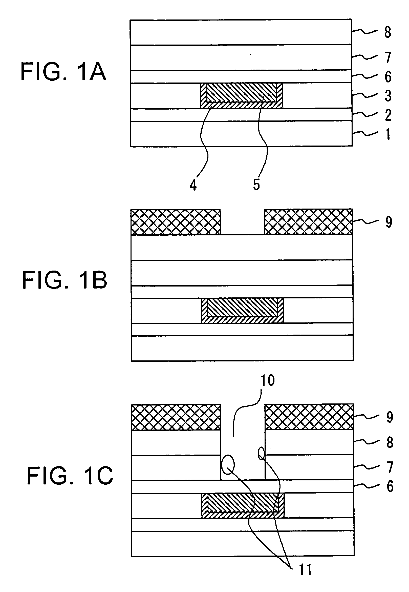
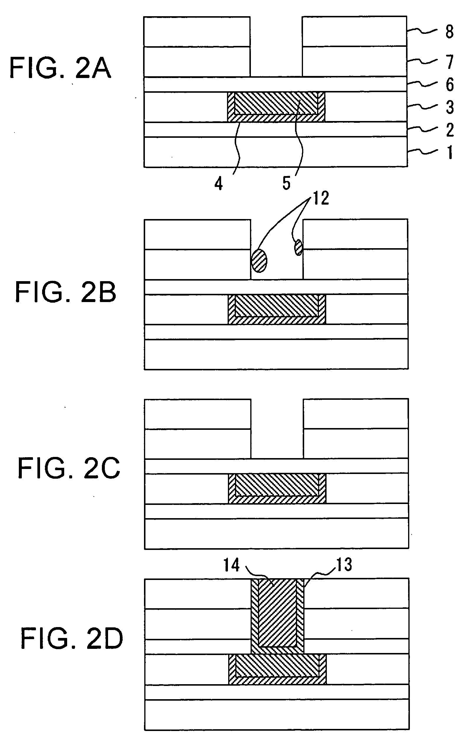
[0086] The embodiment illustrates the case where a transistor is formed in a device formation region of a substrate and the substrate is rinsed using the method according to the invention after formation of a gate of the transistor. A process according to the present embodiment will be described with reference to FIGS. 7A-D and 8A-D.

[0087] First, as shown in FIG. 7A, a silicon substrate 50 is thermally oxidized to form a silicon oxide film 52 on the silicon substrate 50 and a high dielectric constant (high-k) insulating film 54 is deposited thereon by CVD or sputtering, and further, a polysilicon layer 56 is deposited thereon by CVD.

[0088] Subsequently, a resist film is coated on the polysilicon layer 56 and patterned by a lithography technique using ArF excimer laser to form a resist layer 58, as shown in FIG. 7B. Thereafter, as shown in FIGS. 7C and 7D, the polysilicon layer 56 and high-k insulating film 54 are selectively dry-etched in this order using the res...

third embodiment

3. THIRD EMBODIMENT

[0095] The embodiment illustrates the case where a transistor is formed in an I / O region of a substrate and the substrate is rinsed using the method according to the invention after formation of a gate of the transistor. A process according to the embodiment will be described with reference to FIGS. 9A, 9B and 10A-C.

[0096] First, as shown in FIG. 9A, a silicon substrate 50 is thermally oxidized to form a silicon oxide film 52 on the silicon substrate 50 and a high-k insulating film 54 is deposited thereon by CVD or sputtering, and further, a polysilicon layer 56 is deposited thereon by CVD.

[0097] Subsequently, a resist film is coated on the polysilicon layer 56 and patterned by a lithography technique using an I-beam (365 nm) to form a resist layer 65, as shown in FIG. 9B. Thereafter, the polysilicon layer 56, high-k insulating film 54 and the silicon oxide film 52 are selectively dry-etched using the resist layer 65 as a mask to form a gate electrode (FIG. 10A).

[...

example

[0101] In the example, a lower interconnect line made of copper and an upper interconnect line made of copper were connected through a via plug by a single damascene process to form a two level interconnect structure were and then the yield of chips each containing the two level interconnect structure is evaluated. In forming the interconnect structure, wafers to be evaluated were rinsed in various manners after formation of through-holes and removal of resist, and then, the wafers were evaluated in terms of how the rinse affect the yield of chips each containing the interconnect structure.

[0102] Samples for evaluation were manufactured in the following manner. A lower interconnect line and a via plug were formed in the manner similar to that described in the First Embodiment. First, a copper interconnect was formed on a silicon wafer. Then, a silicon nitride film having a thickness of 90 nm, a low-k film having a thickness of 450 nm and a silicon oxide film having a thickness of 45...


PUM

PropertyMeasurementUnit
speedaaaaaaaaaa
thicknessaaaaaaaaaa
thicknessaaaaaaaaaa

Abstract

The stripping agent is sprayed from the tip of the nozzle 33 onto the wafer surface, while the first supply nozzle 33 is actuated to scan from the central portion of the wafer to the outer portion thereof. This operation provides the situation, in which the interface of the residual droplet 38 is pulled back from the center of the wafer to the outer portion of the wafer by the surface tension of the stripping agent supplied from the nozzle. Meanwhile, the second supply nozzle 36 also scans at a same scanning speed as the first supply nozzle 33 scans. Vapor IPA is sprayed from the orifice of the second supply nozzle 36. This provides that vapor IPA is sprayed onto the wafer surface immediately after the stripping agent is sprayed thereon from the first supply nozzle 33, and the residual stripping agent on the wafer surface is efficiently replaced with IPA.

Description

[0001] This application is based on Japanese patent application NO.2002-303629, the content of which is incorporated hereinto by reference.[0002] 1. Field of the Invention[0003] The present invention relates to a technique for cleaning a semiconductor substrate.[0004] 2. Description of the Related Art[0005] Formation of a through-hole or an interconnect trench in a manufacturing process for LSI is generally carried out using a lithography technique and a cleaning technique. A typical process includes steps of: forming a resist pattern on an insulating layer and subsequently dry-etching the insulating layer using the resist pattern as a mask; and then removing the resist pattern by ashing the resist pattern and spraying a stripping solution onto the resist pattern. Further, a rinse is then carried out using a selected solvent. The rinse is carried out to remove residual materials resulting from the resist removal in order to keep the substrate surface clean and thus the rinse is the ...

Claims


Application Information

Patent Timeline
Patent Type & Authority Applications(United States)
IPC IPC(8): H01L21/304B08B3/02B08B3/08H01L21/00H01L21/02H01L21/306H01L21/311H01L21/3213
CPCB08B3/02B08B3/08H01L21/02071Y10S134/902H01L21/31138H01L21/67051H01L21/31116
Inventor AOKI, HIDEMITSUKASAMA, YOSHIKOSUZUKI, TATSUYA
Owner RENESAS ELECTRONICS CORP
Why Eureka
Try Eureka