Optical signal processing element using saturable absorber and optical amplifier

a technology of optical amplifier and optical signal processing element, which is applied in optics, electromagnetic transmission, instruments, etc., can solve the problems of large number of channels used, high power of input optical signal, and very restricted input optical power dynamic range, so as to improve output optical power and eliminate noise. , the effect of improving the extinction ratio

Inactive Publication Date: 2004-04-22
ELECTRONICS & TELECOMM RES INST
View PDF6 Cites 6 Cited by
  • Summary
  • Abstract
  • Description
  • Claims
  • Application Information

AI Technical Summary

Benefits of technology

0012] It is therefore an object of the present invention to provide a new optical signal processing element in which a saturable absorber and a semiconductor optical amplifier are integrated to be capable of amplifying an optical signal, eliminating a noise, increasing an output optical power, improving an extinction ratio, and performing various functions of equalization of output power, wavelength converting, reshaping and reamplifying the output optical signal.

Problems solved by technology

The capacity of an optical communication system based on the wavelength division multiplexing (WDM) method is generally restricted by the number of channels to be used.
Since the cross-gain modulation (XGM) method uses a gain saturation of the semiconductor optical amplifier, there have been problems that a power of the input optical signal should be high and a converted signal has been inverted with respect to an original signal.
The continuous wave is recombined and interferes at Y-combiner either constructively or destructively depending on the bias currents of semiconductor optical amplifier as well as the optical power of the modulated input signal.
However, in the XPM method, since the power of the output optical signal is varied depending on the power of the input optical signal, there has been a problem that the input optical power dynamic range is very restricted.

Method used


Image

  • Optical signal processing element using saturable absorber and optical amplifier
  • Optical signal processing element using saturable absorber and optical amplifier
  • Optical signal processing element using saturable absorber and optical amplifier

Examples


first embodiment

[0028] (First Embodiment)

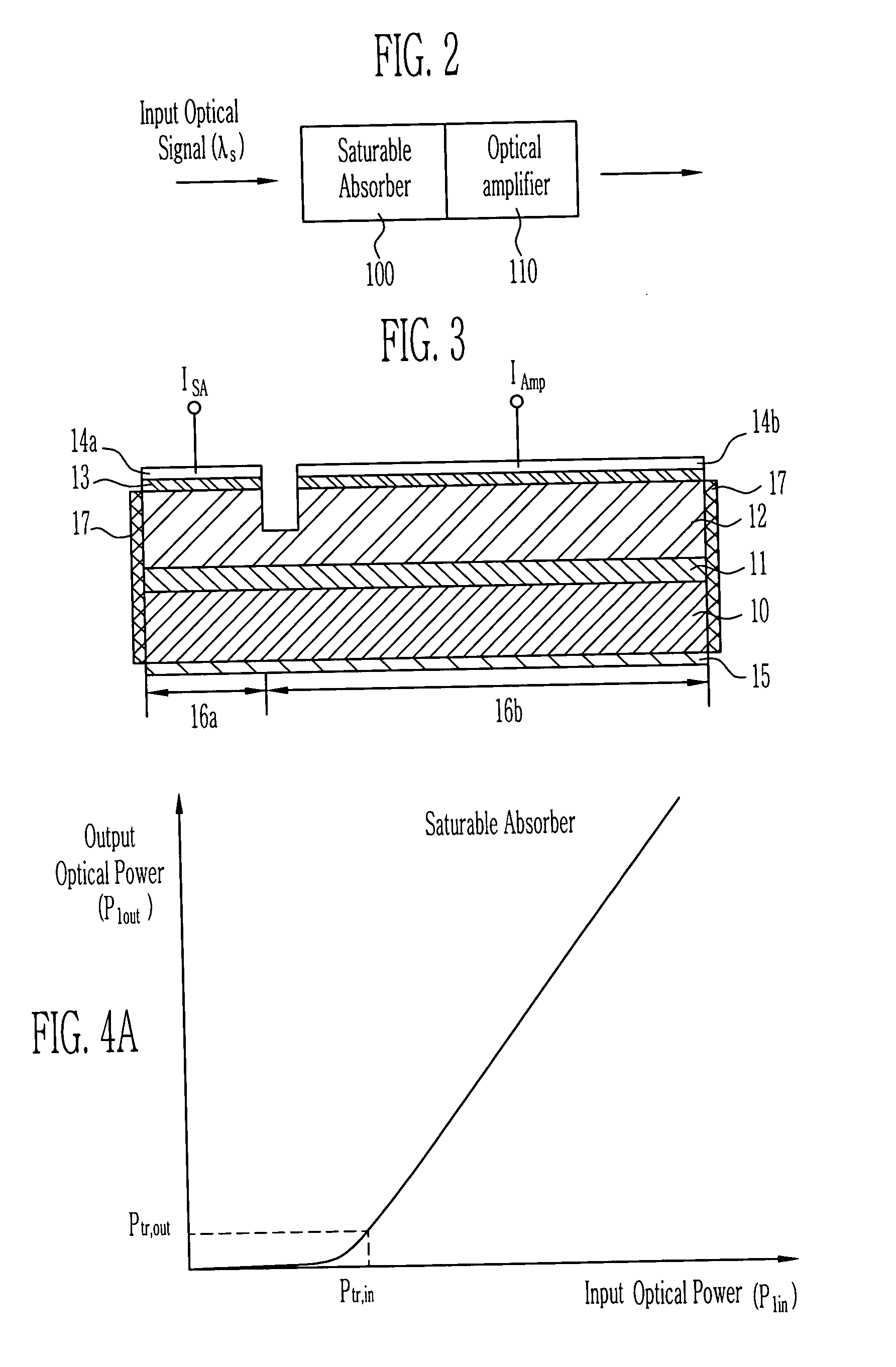
[0029] FIG. 2 is a constructional view illustrating an optical signal processing element according to a preferred embodiment of the present invention. The optical signal processing element comprises a saturable absorber 100 and an optical amplifier 110. FIG. 3 is a longitudinal view illustrating an example of modulating the optical signal processing element in FIG. 2.

[0030] Referring to FIG. 3, the optical signal processing element comprises a saturable absorber area 16a and an optical amplifier area 16b. Upper metal electrodes 14a, 14b are electrically disconnected correspondingly to the saturable absorber area 16a and the optical amplifier area 16b, respectively, and a lower metal electrode 15 is formed all over the saturable absorber area 16a and the optical amplifier area 16b. That is, the optical signal processing element comprises a undoped-doped InGaAsP group active layer 11, a p-doped InP cladding layer 12, an InGaAs ohmic contact layer 13, the upper...

second embodiment

[0040] (Second Embodiment)

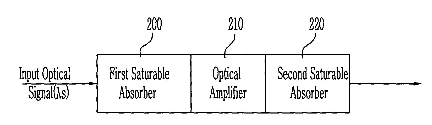
[0041] Now, a second embodiment of the present invention will be described with reference to FIG. 5. FIG. 5 is a constructional view of the optical signal element according to the second embodiment of the present invention. According to the second embodiment of the present invention, as shown in FIG. 5, saturable absorbers 200, 220 may be integrated at both ends of the semiconductor optical amplifier 210. By means of this configuration, it is possible to minimize the noise by reducing the amplified spontaneous emission (ASE) noise generated in the optical signal processing element. In this case, it is preferable that the transparent output optical power of the first saturable absorber 200 is higher than the saturation input optical power of the optical amplifier, and the transparent input optical power of the second saturable absorber 220 is lower than the transparent input optical power of the first saturable absorber 200.

third embodiment

[0042] (Third Embodiment)

[0043] Now, a third embodiment of the present invention will be described with reference to FIGS. 6 and 7.

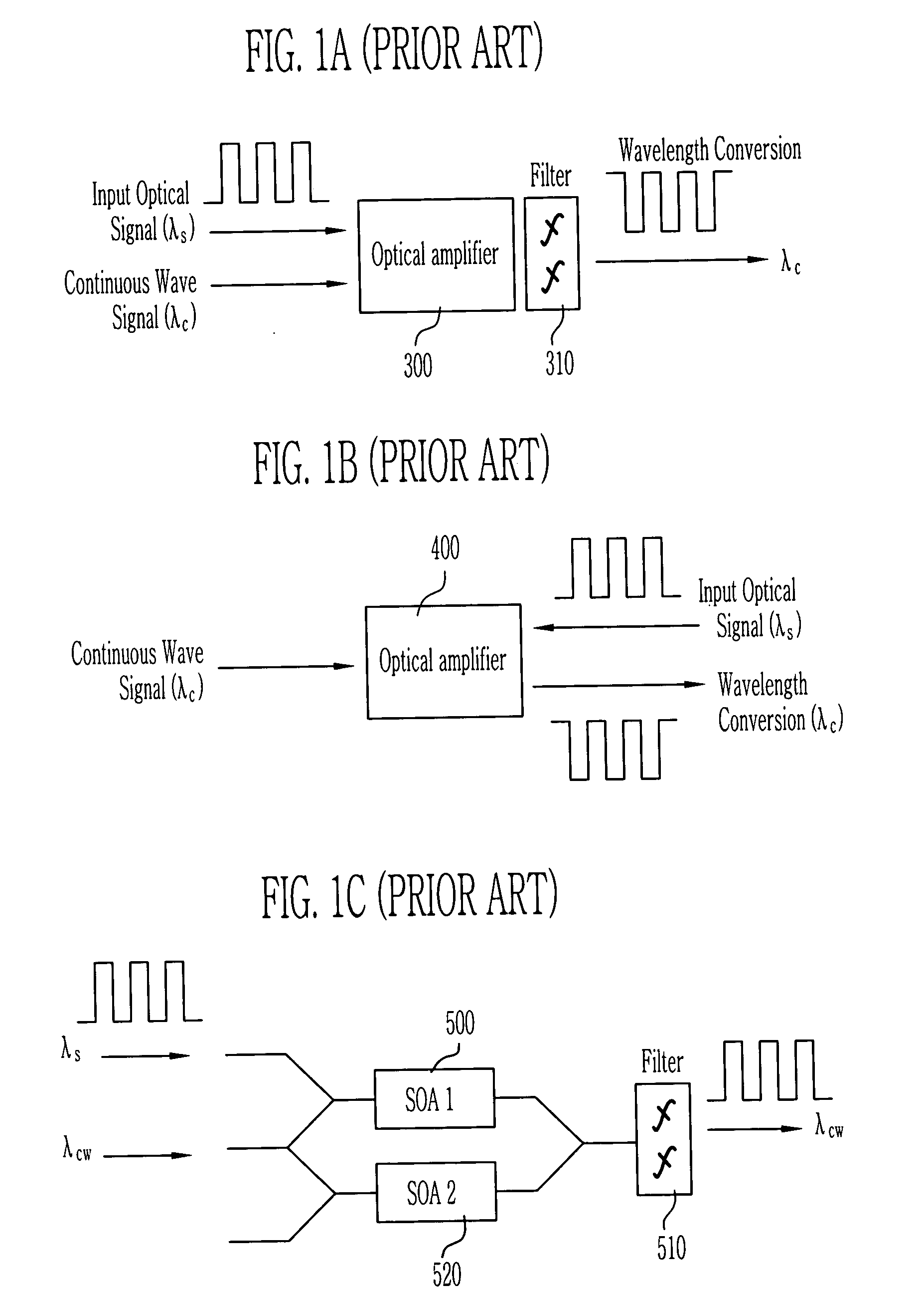
[0044] FIG. 6 is a constructional view of the wavelength converter fabricated using the saturable absorber integrated optical amplifier. The wavelength converter according to this embodiment comprises a saturable absorber 600, an optical amplifier 610 and a filter 620. Now, the operational principle of the wavelength converter will be described with reference to the FIGS. 7A.about.7F. In FIG. 7A, .lambda..sub.c indicates a desired wavelength of the continuous wave, and P.sub.tr indicates the transparent input optical power of the saturable absorber. In FIG. 7B, .lambda..sub.s is indicates the modulated input optical signal. In this case, when both of the modulated input optical signal having the wavelength .lambda..sub.s and the continuous wave signal having the desired wavelength .lambda..sub.c are inputted to the saturable absorber, the modulated input...


PUM

PropertyMeasurementUnit
wavelength bandaaaaaaaaaa
transparentaaaaaaaaaa
optical saturationaaaaaaaaaa

Abstract

The present invention relates to an optical signal processing element capable of performing various functions of equalization of output power, wavelength converting, reshaping or reamplifying an input optical signal using an optical amplifier in which saturable absorbers are integrated, the saturable absorbers being used as an optical gate to improve the extinction ratio of the input optical signal. The saturable absorber and the optical amplifier are connected in series, and a transparent output optical power outputted from the saturable absorber is not less than a saturation input optical power of the optical amplifier.

Description

[0001] 1. Field of the Invention:[0002] The present invention relates to an optical signal processing element used as a key part of a wavelength division multiplexing optical transmission and switching system, and more particularly to an optical signal processing element capable of performing various functions of equalization of output power, wavelength converting, reshaping and reamplifying an input optical signal using an optical amplifier in which saturable absorbers are integrated, the saturable absorber is used as an optical gate to improve an extinction ratio of the input optical signal.[0003] 2. Description of the Prior Art:[0004] Generally, the saturable absorber has been often used in a pulse laser such as a mode locking laser diode disclosed in IEE Electron. Lett., 26, 1087 (1990) by S. Sanders et al., and is recently adapted for a noise elimination disclosed in CLEO, 329 (2000) by Z. Bakonyi et al. and an optical discrimination disclosed in IEE Electron. Lett., 34, 198 (1...

Claims


Application Information

Patent Timeline
Patent Type & Authority Applications(United States)
IPC IPC(8): G02F2/00G02F2/02H01S3/00
CPCG02F2002/006G02F2/004G02F2/006G02F2/02
Inventor KIM, HYUN SOOKIM, JONG HOISIM, EUN DEOKKIM, KANG HOKWON, OH KEEOH, KWANG RYONG
Owner ELECTRONICS & TELECOMM RES INST
Why Eureka
Try Eureka