Buffer layers and articles for electronic devices

Inactive Publication Date: 2004-06-24
UT BATTELLE LLC
View PDF3 Cites 19 Cited by
  • Summary
  • Abstract
  • Description
  • Claims
  • Application Information

AI Technical Summary

Benefits of technology

0008] Accordingly, it is an object of the present invention to provide new and improved materials and methods for depositing buffer layers on biaxially textured and untextured metallic and metal oxide substrates for use in the manufacture of superconducting and other electronic articles. It is a further object to provide new and improved mater

Problems solved by technology

However, many buffer layer materials or substrates exhibit a deleterious chemical reactivity toward the precursor layer during the ex situ anneal to the extent that

Method used


Image

  • Buffer layers and articles for electronic devices
  • Buffer layers and articles for electronic devices
  • Buffer layers and articles for electronic devices

Examples


example ii

Growth of LMO on a Metallic Substrate by Sputtering Followed by YBCO Deposition

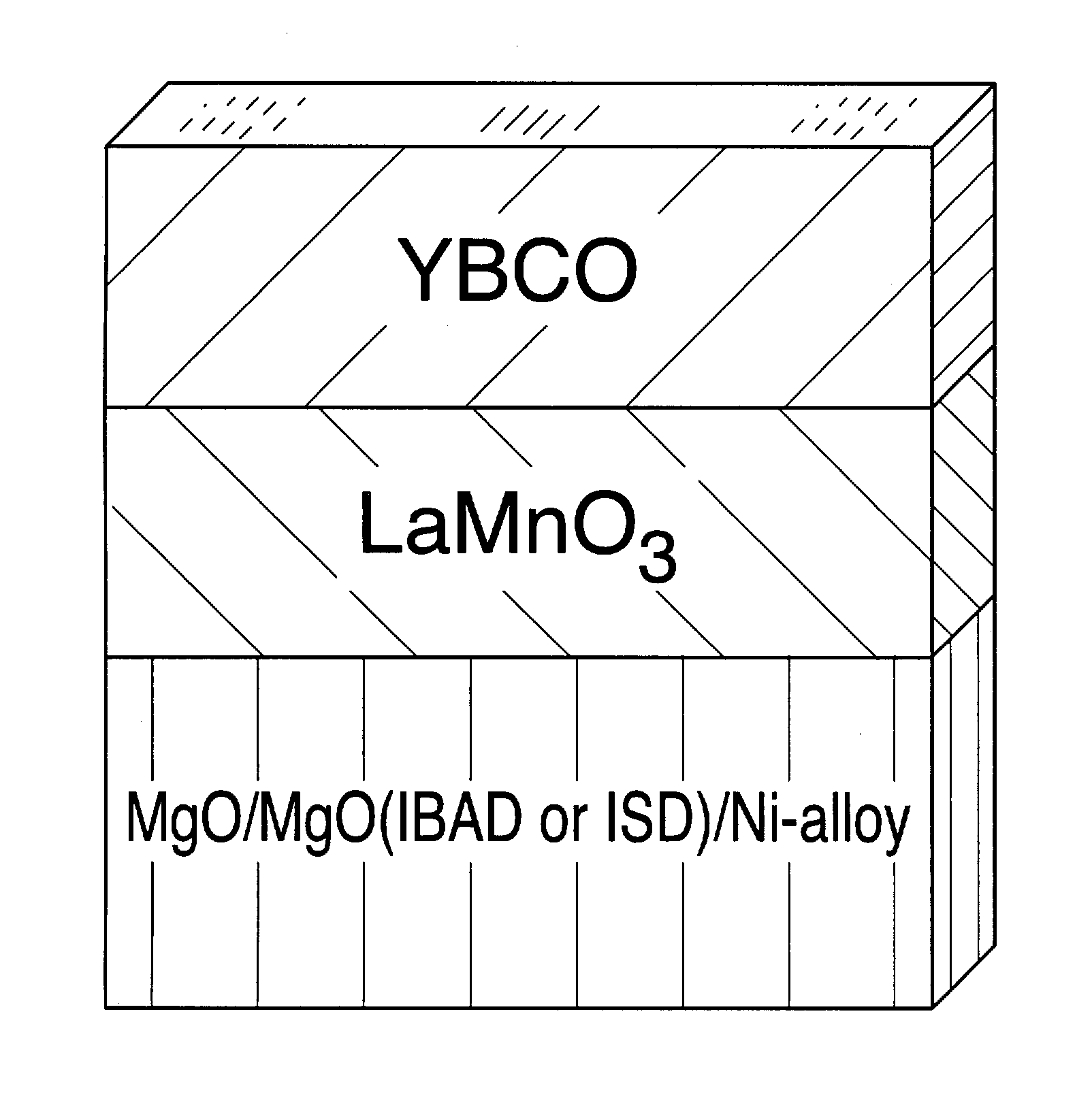
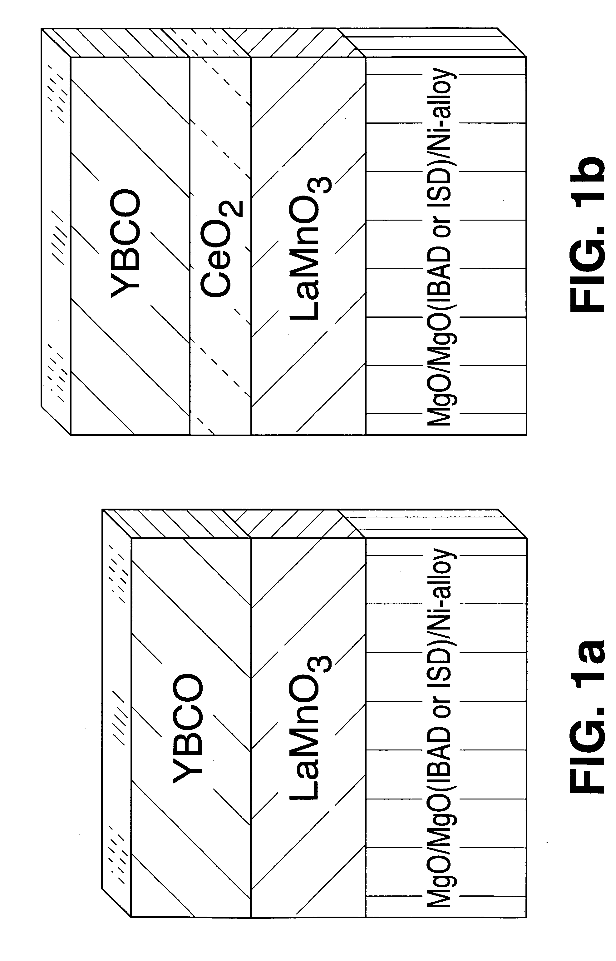
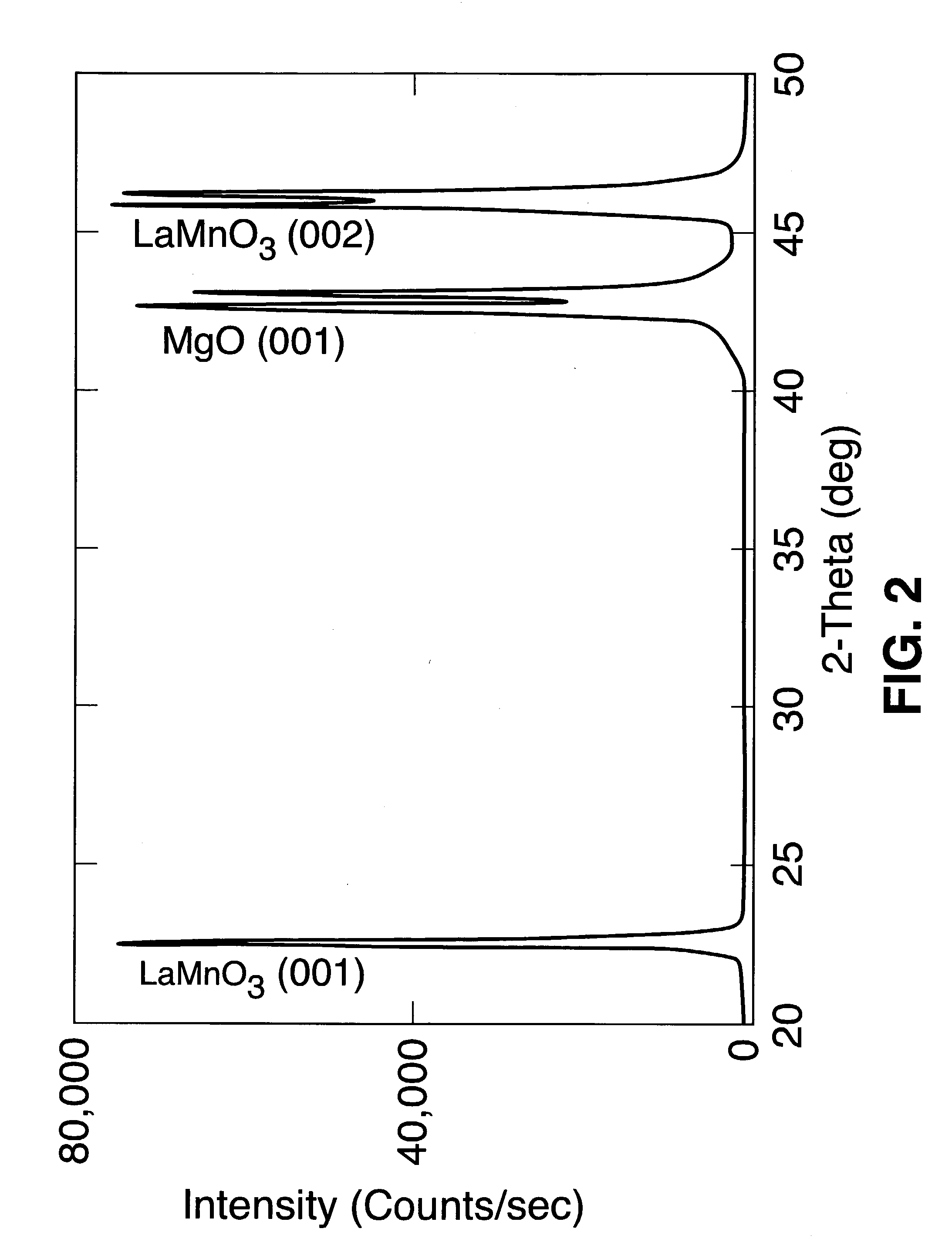
[0036] In this example, the development of a suitable buffer layer architecture for YBa.sub.2Cu.sub.3O.sub.7 (YBCO) coated conductors using the BF method to produce the YBCO is described. The architecture comprises LMO, as a buffer layer between the YBCO and a metallic substrate or a metallic substrate coated with a suitably selected additional buffer layer or buffer layer stack. The YBCO is deposited and epitaxially grown directly onto the LMO. To test the compatibility of LMO, a substrate was provided consisting of biaxially textured, rolled Ni tape coated with an epitaxial Gd.sub.2O.sub.3 buffer layer. A dense and crack-free layer of LMO was grown epitaxially onto the Gd.sub.2O.sub.3. A YBCO layer with a thickness of 0.3 .mu.m then was grown onto the LMO using the BF method. First a non-superconducting precursor layer was deposited onto the LMO by electron-beam co-evaporation of Y, BaF.sub.2, and Cu. T...

example iii

Growth of RMnO.sub.3 on Textured Substrates Where R Comprises at Least One of Ce. Pr, Nd, Pm, Sm, Eu, Gd, Th, Dy, Ho, Er, Tm, Yb, Lu, and Y

[0044] Very recent reports indicate and confirm that many new compounds besides LMO exist in the general chemical formula RMnO.sub.3, where R can be Ce, Pr, Nd, Pm, Sm, Eu, Gd, Tb, Dy, Ho, Er, Tm, Yb, Lu, or Y. RMnO.sub.3 compounds crystallize in orthorhombic structure [space group Pbnm (D.sup.16.sub.2h) and Z=4] for R with larger ionic radius where R may be La, Ce, Pr, Nd, Pm, Sm, Eu, Gd, Th, or Dy. For further details, refer to L. Martin-Carron, A. de Andres, M. J. Martiniz-Lope, M. T. Casais, and J. A. Alonso, J. of Alloy and Compounds, 323-324 (2001) 494-497. For this set, the ionic radius varies between 1.15 .ANG. and 0.99 .ANG..

[0045] For compounds with smaller ionic radius (R may be Ho, Er, or Y), either the orhorhombic or the hexagonal structure [space group P6.sub.3cm(C.sup.3.sub.6v) and Z=7] can be obtained. For further details, refer t...

example iv

Growth of MgO on a Biaxially Textured Metal Substrate by e-beam Evaporation Followed by LaMnO.sub.3 (Using Sputtering) and YBCO Deposition

[0051] An electron beam (e-beam) evaporation technique was used to deposit Magnesium Oxide, MgO films directly on biaxially textured Cu or Cu-alloys or Ni or Ni-alloys. The as-rolled Cu substrates were cleaned ultrasonically with both acetone and methanol and recrystallized to the desired {100} cube texture by annealing the substrates at 800.degree. C. for 1 hour in a vacuum of 10.sup.-6 Torr. Biaxially oriented Cu substrates were mounted on a substrate holder with a heater assembly in the e-beam system. After the vacuum in the chamber had reached 1.times.10.sup.-6 Torr at room temperature, the substrate was then heated in the range of 300 to 700.degree. C. and MgO layers were deposited at that temperature. The preferred deposition temperature is about 400.degree. C. After the deposition, the film was heated to about 600.degree. C. and cooled to r...


PUM


Abstract

Materials for depositing buffer layers on biaxially textured and untextured metallic and metal oxide substrates for use in the manufacture of superconducting and other electronic articles comprise RMnO3, R1-xAxMnO3, and combinations thereof; wherein R includes an element selected from the group consisting of La, Ce, Pr, Nd, Pm, Sm, Eu, Gd, Th, Dy, Ho, Er, Tm, Yb, Lu, and Y, and A includes an element selected from the group consisting of Be, Mg, Ca, Sr, Ba, and Ra.

Description

[0002] The present invention relates to materials and methods for depositing buffer layers on biaxially textured and untextured metallic and metal oxide substrates for use in the manufacture of superconducting and other electronic articles, and more particularly to substrates comprising RMnO.sub.3, R.sub.1-xA.sub.xMnO.sub.3, and combinations thereof, wherein R comprises an element selected from the group consisting of La, Ce, Pr, Nd, Pm, Sm, Eu, Gd, Th, Dy, Ho, Er, Tm, Yb, Lu, and Y, and A comprises an element selected from the group consisting of Be, Mg, Ca, Sr, Ba, and Ra.[0003] One standard architecture for the ion-beam assisted deposition (IBAD) based Y--Ba.sub.2--Cu.sub.3--O.sub.x (YBCO) coated conductors utilizing CeO.sub.2, yttria stabilized zirconia (YSZ), and MgO is YBCO / CeO.sub.2 / YSZ / MgO(IBAD) / Ni-alloy. Since very thin MgO (IBAD) layers are sufficient to get the necessary biaxial texture, it is essential to provide a simplified buffer layer architecture to grow YBCO films....

Claims


Application Information

Patent Timeline
IPC IPC(8): B32B9/00B32B9/04B32B15/04H01L39/24
CPCC30B23/02H01L39/2461C30B29/24C30B29/225H10N60/0632
Inventor PARANTHAMAN, MARIAPPAN P.AYTUG, TOLGACHRISTEN, DAVID K.FEENSTRA, ROELANDGOYAL, AMIT
Owner UT BATTELLE LLC
Why Eureka
Try Eureka