Method of forming fine patterns

Inactive Publication Date: 2004-06-24
TOKYO OHKA KOGYO CO LTD
View PDF1 Cites 20 Cited by
  • Summary
  • Abstract
  • Description
  • Claims
  • Application Information

AI Technical Summary

Problems solved by technology

However, in these methods, it is difficult to control the thickness of layers to be formed on the sidewalls of resist patterns.
In addition, the in-plane heat dependency of wafers is as great as ten-odd nanometers per degree Celsius, so it is extremely difficult to keep the in-plane uniformity of wafers by means of the heater employed in current fabrication of semiconductor devices and this leads to the problem of occurrence of significant variations in pattern dimensions.
On the other hand, it is difficult to control the resist deformation and fluidizing on account of heat treatment, so it is not easy to provide a uniform resist pattern in a wafer's plane.
However, the use of polyvinyl alcohol singly is not highly soluble in water and cannot be readily removed completely by washing with water, introducing difficulty in forming a pattern of good profile.
The pattern formed is not completely satisfactory in terms of stability over ti

Method used


Image

  • Method of forming fine patterns
  • Method of forming fine patterns
  • Method of forming fine patterns

Examples


example 1

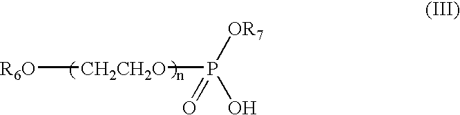
[0068] A copolymer including polyacrylate (PAA) and polyvinylpyrrolidone (PVP) [2 g: PAA / PVP=2:1 (polymerization ratio)], triethanolamine (0.18 g) and a polyoxyethyelene phosphate ester surfactant (0.02 g; "PLYSURF A210G", product of Dai-ichi Kogyo Seiyaku Co, Ltd.) were dissolved in water (52 g) to prepare an over-coating agent.

[0069] A substrate (8-inch diameter) was whirl coated with a positive-acting photoresist TDUR-PO36PM (product of Tokyo Ohka Kogyo Co., Ltd.) and baked at 80.degree. C. for 90 seconds to form a photoresist layer in a thickness of 0.48 .mu.m.

[0070] The photoresist layer was exposed with an exposure unit (Canon EPA-3000EX3, product of Canon Inc.), subjected to heat treatment at 120.degree. C. for 90 seconds and developed with an aqueous solution of 2.38 mass % TMAH (tetramethylammonium hydroxide) to form photoresist patterns which defined hole patterns with an each diameter of 178.9 nm (i.e., the spacing between the photoresist patterns, or the initial hole dim...

example 2

[0072] The same procedure as described in Example 1 was repeated, except that the substrate was brought into contact with pure water by dropping it on the substrate for 90 seconds. Each diameter of the hole patterns was narrowed to 158.3 nm, and few defects were occurred on the entire substrate


PUM


Abstract

It is disclosed a method of forming fine patterns comprising: covering a substrate having photoresist patterns with an over-coating agent for forming fine patterns, applying heat treatment to cause thermal shrinkage of the over-coating agent so that the spacing between adjacent photoresist patterns is lessened by the resulting thermal shrinking action, and removing the over-coating agent substantially completely by way of bringing thusly treated substrate into contact with a remover solution for over 60 seconds.

Description

BACKGROUND OF THE INVETNION[0001] 1. Field of the Invention[0002] This invention relates to a method of forming fine patterns in the field of photolithographic technology. More particularly, the invention relates to a method of forming or defining fine patterns, such as hole patterns and trench patterns, that can meet today's requirements for higher packing densities and smaller sizes of semiconductor devices.[0003] 2. Description of the Related Art[0004] In the manufacture of electronic components such as semiconductor devices and liquid-crystal devices, there is employed the photolithographic technology which, in order to perform a treatment such as etching on the substrate, first forms a film (photoresist layer) over the substrate using a so-called radiation-sensitive photoresist which is sensitive to activating radiations, then performs exposure of the film by selective illumination with an activating radiation, performs development to dissolve away the photoresist layer selecti...

Claims


Application Information

Patent Timeline
IPC IPC(8): G03F7/40H01L21/027
CPCH01L21/0274G03F7/40H01L21/027
Inventor KANEKO, FUMITAKESUGETA, YOSHIKITACHIKAWA, TOSHIKAZU
Owner TOKYO OHKA KOGYO CO LTD
Why Eureka
Try Eureka