Display device

a display device and display technology, applied in static indicating devices, instruments, non-linear optics, etc., can solve the problems of power consumption increase, voltage required for driving liquid crystals cannot be stored, and capacitor lines may not necessarily be provided

Inactive Publication Date: 2004-07-01
SEMICON ENERGY LAB CO LTD
View PDF8 Cites 12 Cited by
  • Summary
  • Abstract
  • Description
  • Claims
  • Application Information

AI Technical Summary

Problems solved by technology

However, the capacitor line may not necessarily be provided if other wiring and the like can concurrently serve as the capacitor line.
Conventional active matrix display devices suffer from problems in that its display portion has a dynamic RAM (DRAM) structure with a storage capacitor and a switching circuit as described above, thus a periodica

Method used


Image

  • Display device
  • Display device
  • Display device

Examples


embodiment 1

[0056] [Embodiment 1]

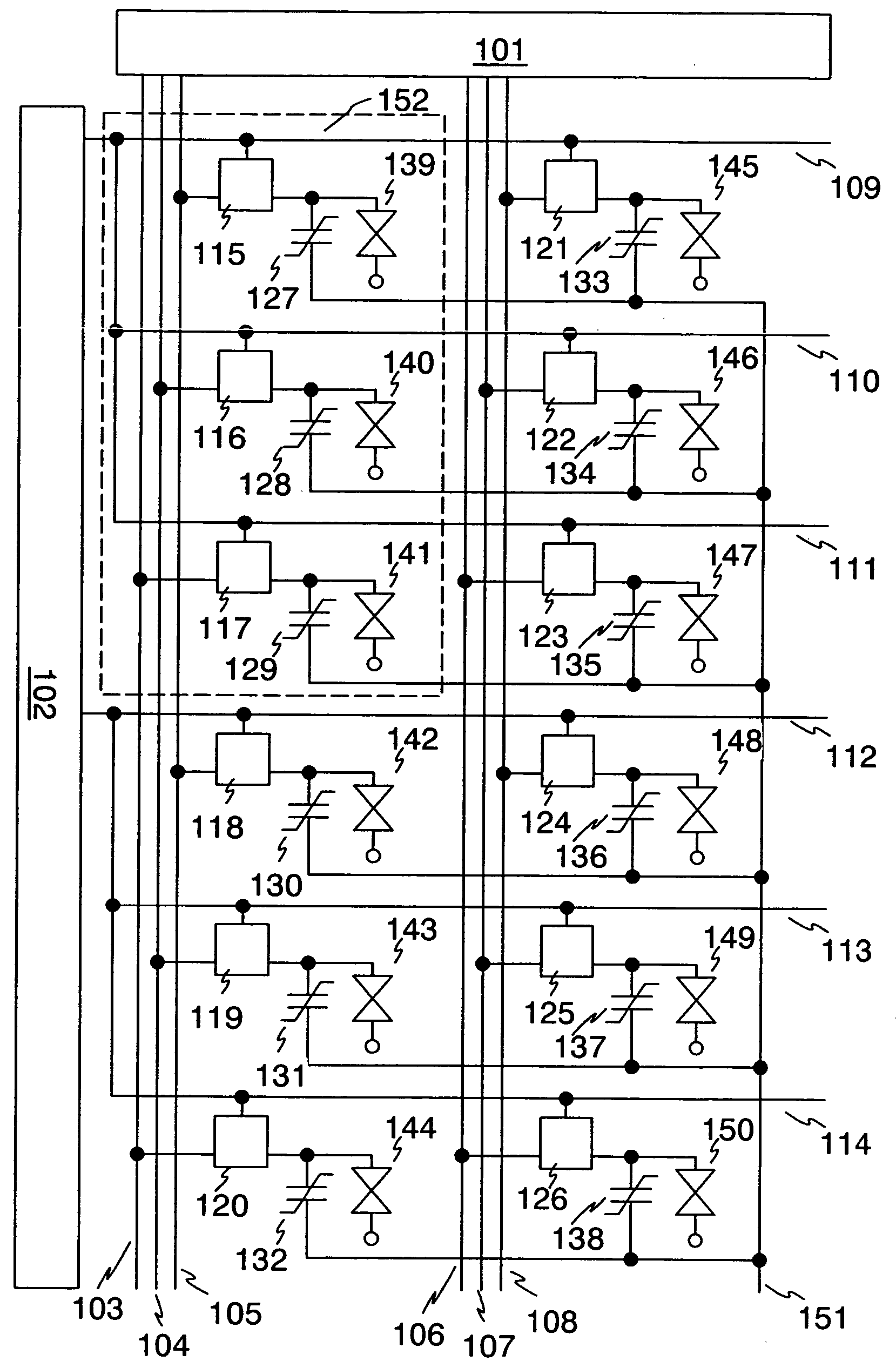
[0057] Shown in FIG. 4 is a configuration of an embodiment of the invention. In this embodiment, switching elements are formed of TFTs. Note that, a 3-bit gradation is taken as an example in FIG. 4, however, the invention is not exclusively limited to 3-bit. One pixel 452 comprises three TFTs and three nonvolatile memory elements. ON / OFF operations of the TFTs are controlled by gate signal lines. One terminal of each nonvolatile memory element is connected to each TFT and to each liquid crystal element via a pixel electrode (not shown in the figure), and the other terminal thereof is connected to a common electrode 451. Operation thereof is explained below.

[0058] Digital video signals are outputted from a source signal line driver circuit 401 to source signal lines 403 to 408. When gate signal lines 409 to 411 are selected by a gate signal line driver circuit 402, TFTs 415 to 417 and 421 to 423 are turned ON and the digital video signals from the source signal l...

embodiment 2

[0063] [Embodiment 2]

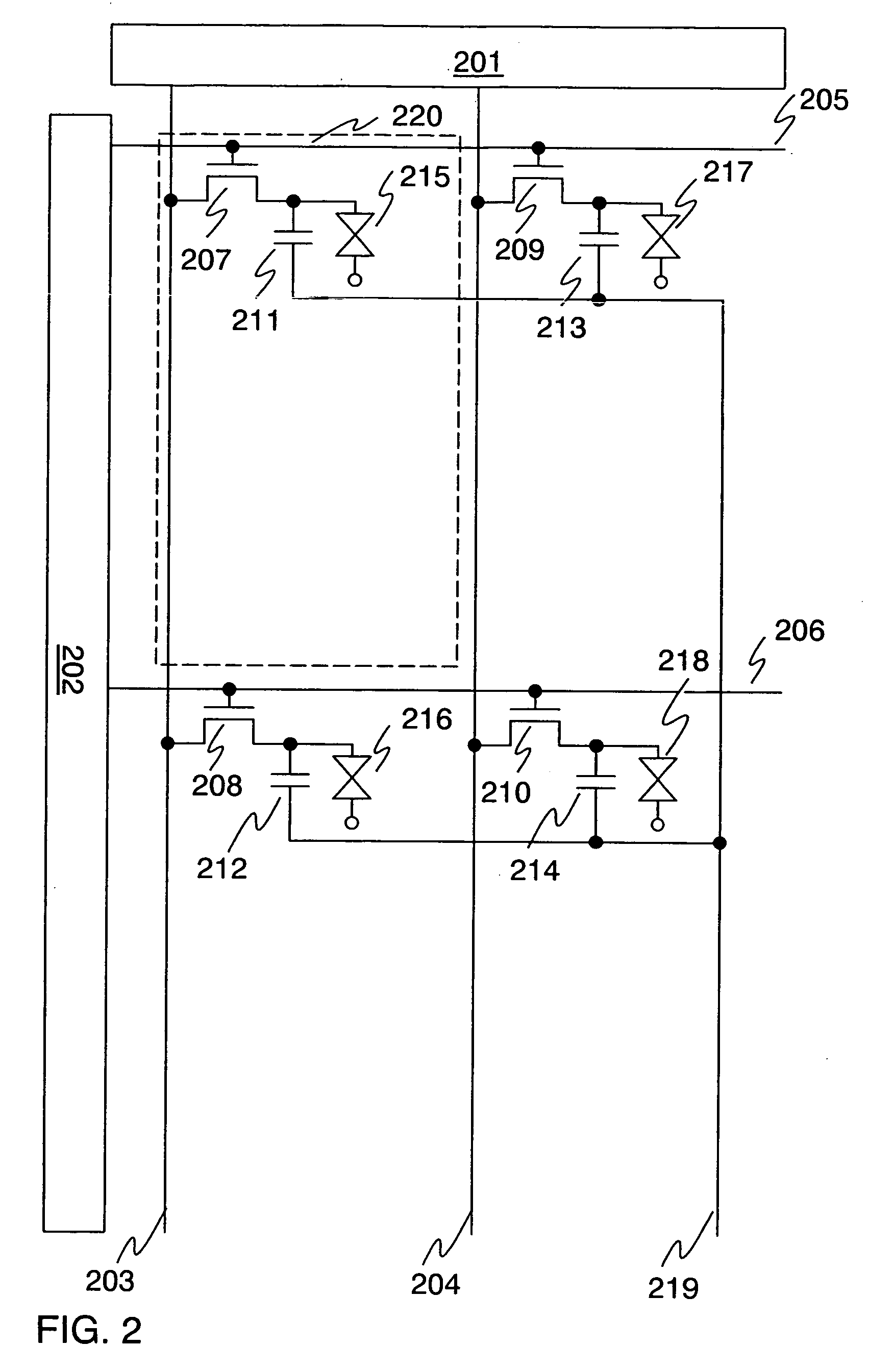
[0064] Shown in FIG. 5 is a configuration of an embodiment of the invention. This embodiment is different from Embodiment 1 in that one source signal line is provided corresponding to one pixel column. Note that, a 3-bit gradation is taken as an example in FIG. 5, however, the invention is not exclusively limited to 3-bit. One pixel 548 comprises three TFTs and three nonvolatile memory elements. ON / OFF operations of the TFTs are controlled by gate signal lines. One terminal of each nonvolatile memory element is connected to each TFT and to each liquid crystal element via a pixel electrode (not shown in the figure), and the other terminal thereof is connected to a common electrode 547. Operation thereof is explained below.

[0065] Digital video signals are outputted from a source signal line driver circuit 501 to source signal lines 503 and 504. When a gate signal line 505 is selected by a gate signal line driver circuit 502, TFTs 515 and 517 are turned ON and the ...

embodiment 3

[0069] [Embodiment 3]

[0070] Shown in FIG. 6 is an embodiment of a source signal line driver circuit which corresponds to the pixel configuration shown in Embodiment 1. In FIG. 6, the source signal line driver circuit comprises a shift register 601, a 1st latch circuit 614, and a 2nd latch circuit 615. Operation of the source signal line driver circuit is explained below.

[0071] When output pulses from the shift register 601 are inputted to latch circuits 602 to 604, digital video signals from a video signal line 616 are stored in the latch circuits 602 to 604. Subsequently, when output pulses from the shift register 601 are inputted to latch circuits 608 to 610, digital video signals from the video signal line 616 are stored in the latch circuits 608 to 610. In this manner, output pulses from the shift register 601 are sequentially scanned and video signals corresponding to one line are stored in the 1st latch circuit 614. Then, before an image of a succeeding line is displayed, latc...


PUM


Abstract

In an active matrix display device using an SRAM, the number of transistors configuring the SRAM circuit is large. Therefore, the transistors cannot be embedded in a pixel when a pixel area is small, otherwise an aperture ratio is reduced. In view of the foregoing, it is an object of the present invention to provide a display device without a refreshing operation and thus with small power consumption. According to the invention, a display device including a pixel which comprises a switching element and a nonvolatile memory element is provided. When a still image is displayed by utilizing a ferroelectric element as a nonvolatile memory element and storing a signal, writing is not required per frame. Further, as the ferroelectric element occupies a small area, a memory circuit can be incorporated without decreasing an aperture ratio.

Description

[0001] 1. Field of the Invention[0002] The present invention relates to a display device, and more particularly to a display device using a thin film transistor (TFT) formed on a transparent substrate such as glass or plastics, and a driving method of the same. In addition, the invention relates to electronic apparatuses using the display device.[0003] 2. Description of the Related Art[0004] In recent years, with the advance of the communication technology, mobile phones have been widely used. In future, transmission of moving images and a larger volume of information are expected. On the other hand, through reduction in weight of personal computers, those adapted for mobile communication have been produced. Information terminals called PDA originated in electronic notebooks have also been produced in large quantities and widely used. In addition, with the development of display devices, the majority of portable information devices are equipped with a flat panel display.[0005] Moreo...

Claims


Application Information

Patent Timeline
IPC IPC(8): G02F1/133G02F1/136G02F1/1362G09G3/20G09G3/32G09G3/36G11C11/22H01L21/77H01L27/105H01L27/12H01L27/13H01L29/786H01L31/109
CPCG02F1/136213G09G3/2074G09G3/3233G09G3/3258G09G3/3648G09G3/3688H01L27/1255G09G2300/0857G09G2300/0876G09G2320/10G11C11/22H01L27/105H01L27/1214G09G2300/0842G02F1/133
Inventor KOYAMA, JUN
Owner SEMICON ENERGY LAB CO LTD
Why Eureka
Try Eureka