Method for manufacturing semiconductor device

US20120171833A1Active Publication Date: 2012-07-05INST OF MICROELECTRONICS CHINESE ACAD OF SCI

Image

  • Method for manufacturing semiconductor device
  • Method for manufacturing semiconductor device
  • Method for manufacturing semiconductor device

Examples


Embodiment Construction

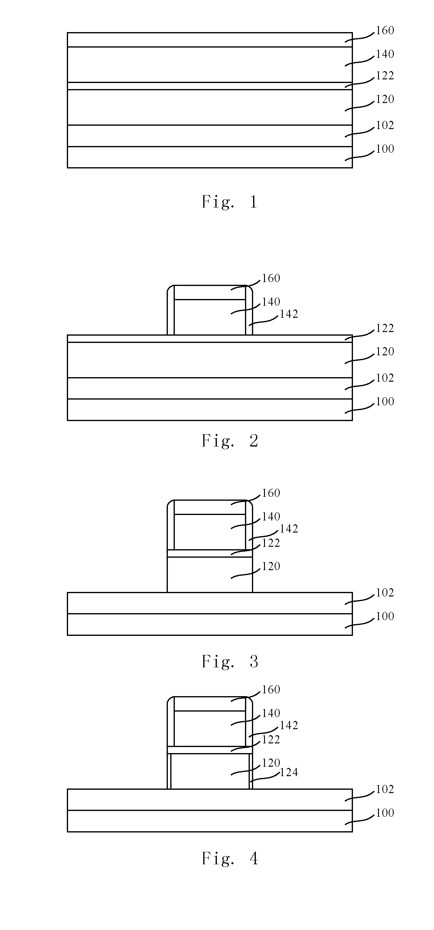
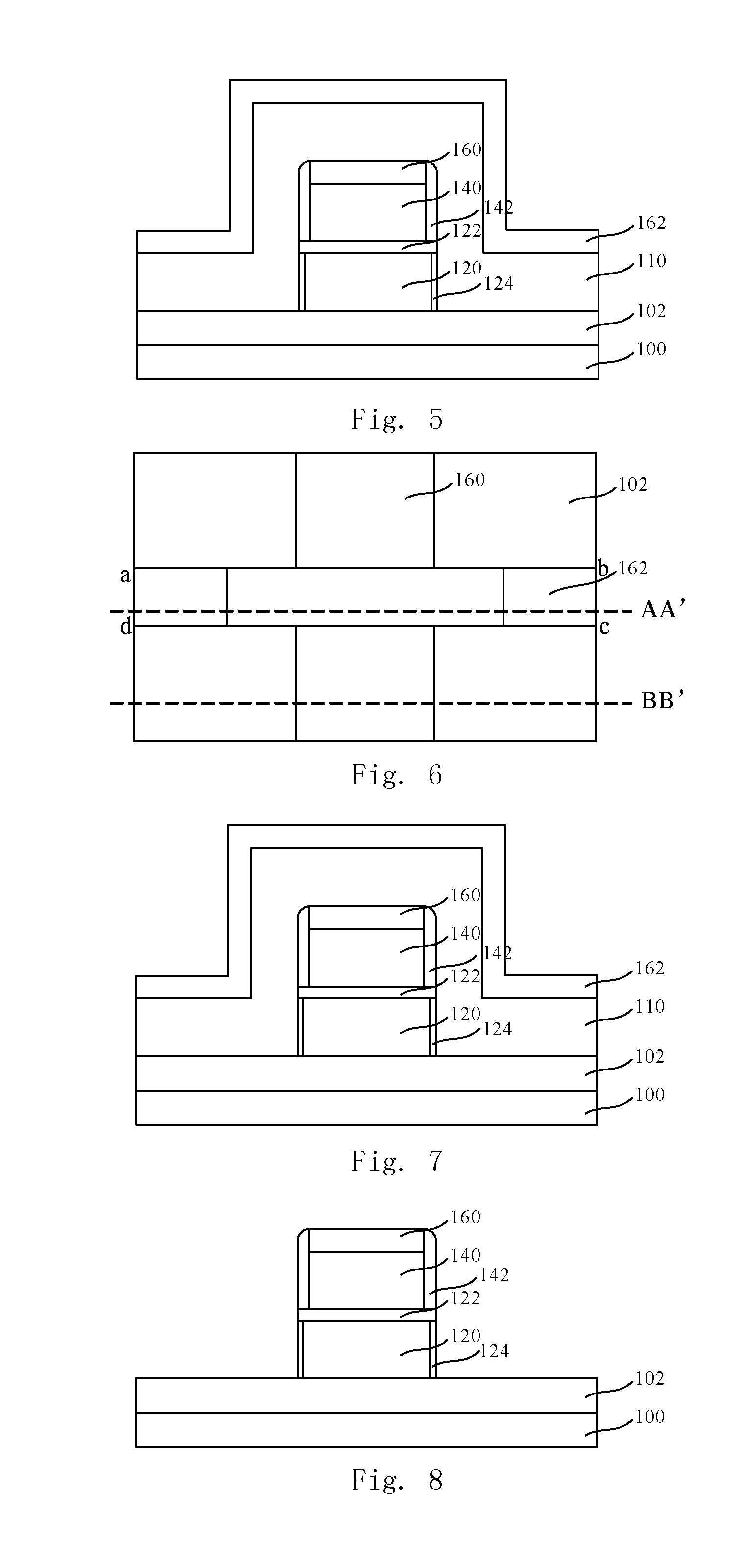
[0044]The disclosure below provides various embodiments or examples for carrying out the technical solution of the present invention. Although the components and arrangements of some specific examples are described, they are only examples, and are not construed as limiting the present invention.

[0045]Moreover, reference numerals and / or letters are repeated in various embodiments. The repetition is for simplicity and clarity, and does not represent relationship between various embodiments and / or settings to be discussed below.

[0046]Various specific processes and / or materials are used in the present invention. Nevertheless, one skilled person in the art will appreciate that other processes and / or materials can also be used as alternatives without departing from the protection scope of the invention. It should be noted that boundaries of various regions described herein include necessary extensions introduced by the process.

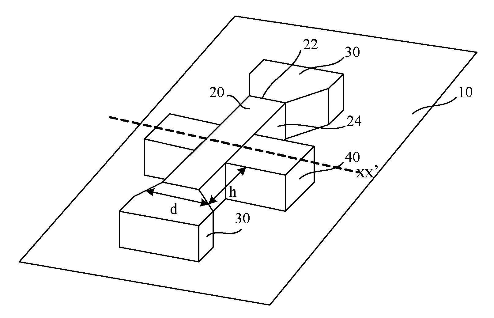
[0047]According to the present invention, there is provided a ...


PUM


Abstract

The present application discloses a method for manufacturing a semiconductor device, comprising the steps of: forming a semiconductor substrate, a gate stack and a second protection layer in sequence on a first insulating layer; after defining a gate region and removing portions of the second protection layer and the gate stack outside the gate region, while keeping portions of the stop layer, the semiconductor layer and the second insulating layer which covers sidewalls of the patterned semiconductor layer outside the gate region and exposing the sacrificial layer, performing source / drain ion implementation in the semiconductor layer; after forming a second sidewall spacer so as to cover at least the exposed portion of the sacrificial layer, removing the first protection layer and the second protection layer so as to expose the semiconductor layer and the gate stack; and forming a contact layer on the exposed portion of the semiconductor layer and the gate stack; performing planarization so as to expose the first protection layer, and then removing the first protection layer, the sacrificial layer, the stop layer and the semiconductor layer with the first sidewall spacer and the second sidewall spacer as a mask, so as to form a cavity which exposes the first insulating layer. It facilitates reduction of short channel effects, resistance of source / drain regions, and parasite capacitance.

Description

FIELD OF THE INVENTION[0001]The present invention relates to semiconductor technology, and particularly, to a method for manufacturing a semiconductor device.BACKGROUND OF THE INVENTION[0002]When the channel length of a metal oxide semiconductor field effect transistor (MOSFET) becomes smaller continuously, many negligible effects in the long-channel model of the MOSFET becomes more significant, and has even been a dominant factor determining its properties. These effects are commonly referred to as short channel effects. The short channel effect deteriorates electrical properties of the device, which, for example, leads to a reduced gate threshold voltage, increased power consumption, and a lowered signal-to-noise ratio.[0003]To suppress the short channel effect, the channel has to be doped with more elements such as phosphorus, boron, and the like, which, however, decreases the carrier mobility in the channel of the device. Moreover, it is difficult to provide a steep doping profi...

Claims


Application Information

Patent Timeline
05 Jul 2012
Publication
US20120171833A1
IPC
H01L29/78
CPC
H01L29/66795
Inventors
ZHU, HUILONG; LI, CHUNLONG