Detection, resolution, and identification of arrayed elements

a technology of arrays and elements, applied in the field of arrays, can solve the problems of large amount of user interaction, large number of arrays, and inability to continue to capture photons, and software is not well suited to analysis of large arrays of elements, and even a limited number of elements

Inactive Publication Date: 2004-10-21
INVERNESS MEDICAL - BIOSTAR
View PDF24 Cites 90 Cited by
  • Summary
  • Abstract
  • Description
  • Claims
  • Application Information

AI Technical Summary

Problems solved by technology
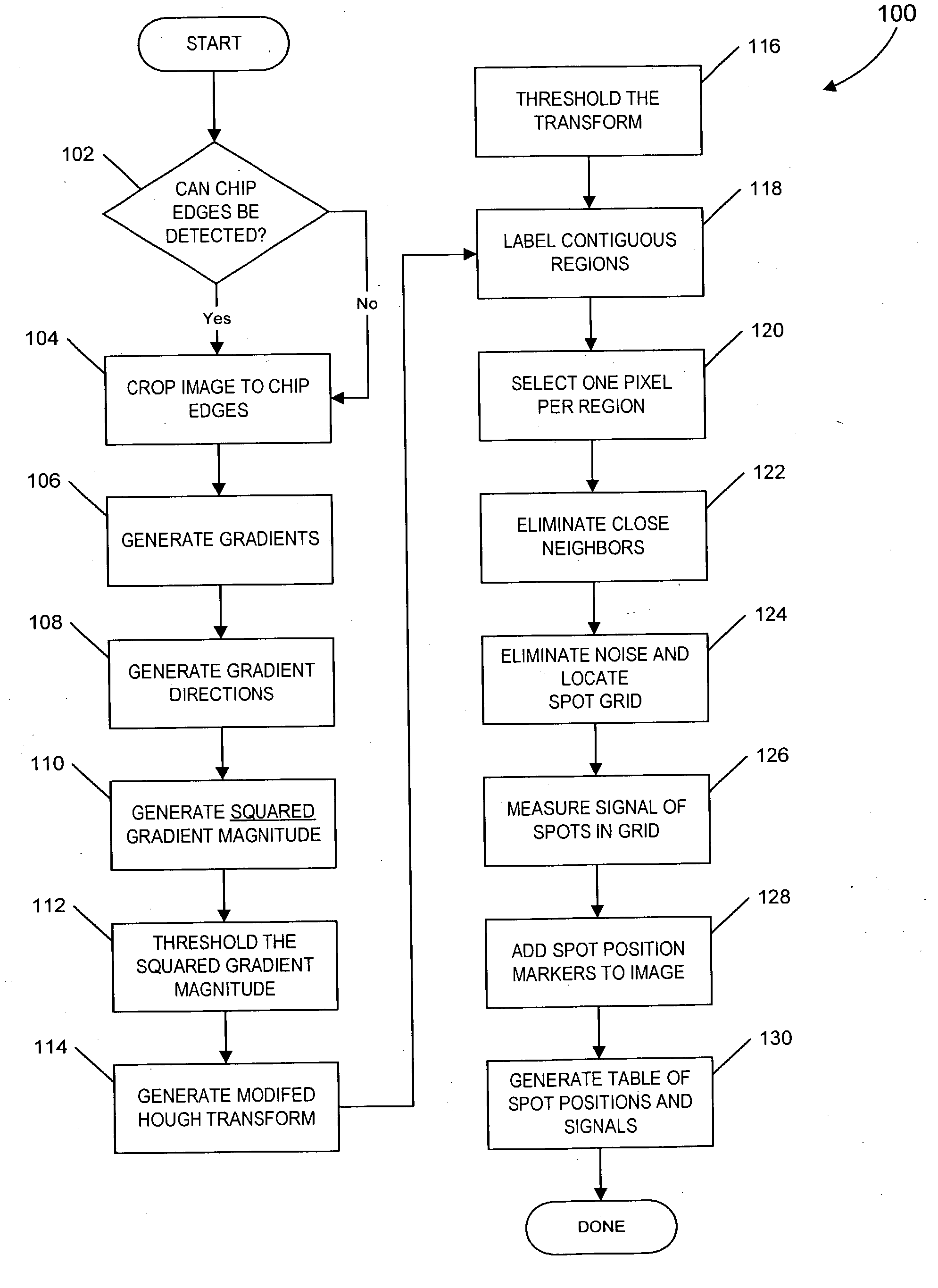
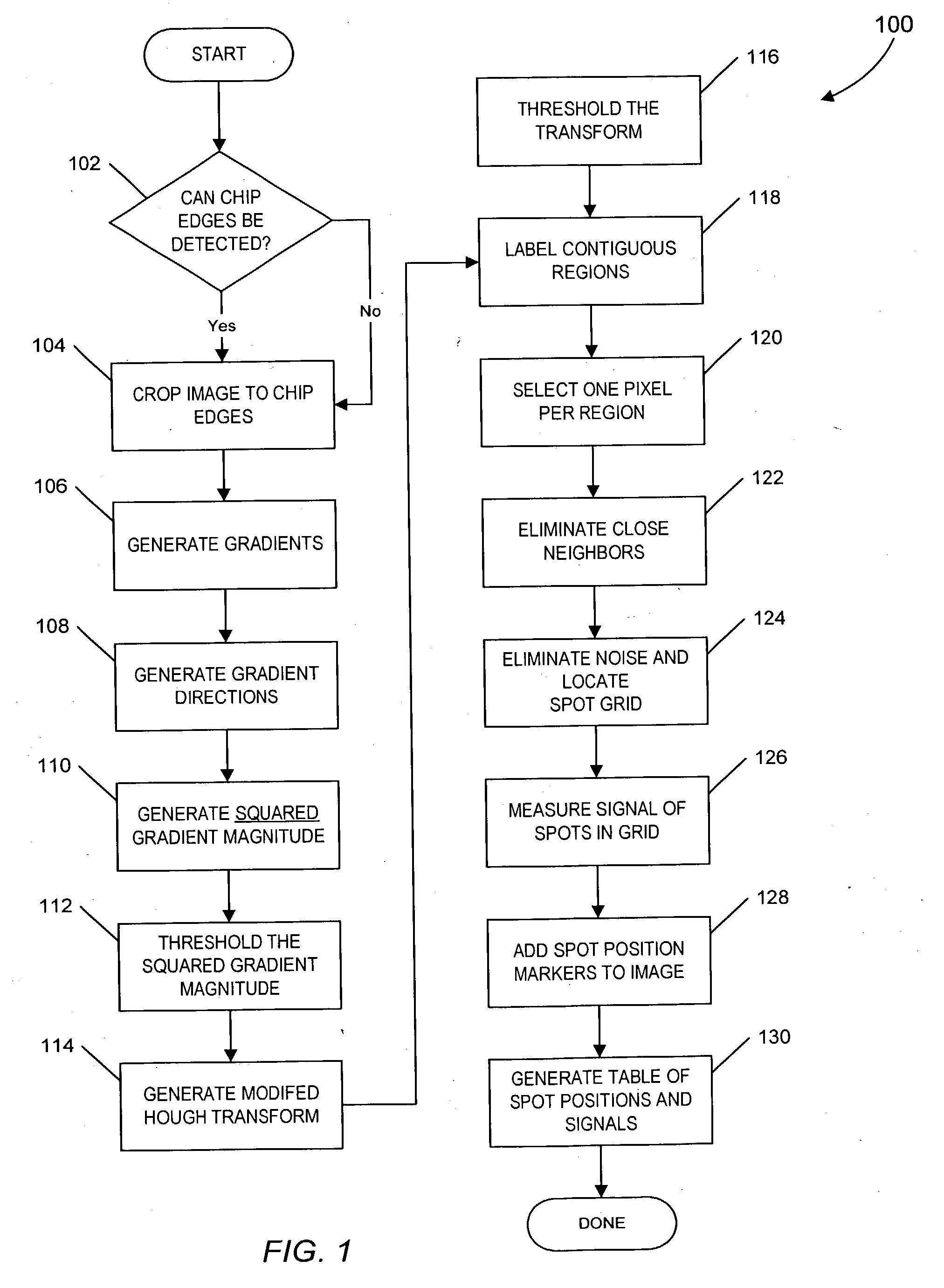
Therefore, when the charge transfer occurs, the pixel is busy and cannot continue to capture photons.
While performance of these existing tools is well suited to analysis of single arrays, even with a large number of elements, they are not well suited to analysis of large numbers of arrays, of even a limited number of elements, with any frequency of analysis.
However, this software requires a large amount of user interaction to analyze even small arrays.
If one assumes a 16-spot 4.times.4 array, each corner spot will also be indistinguishable from any other corner spot; thus, determining the proper "upper left" location of the array may be impossible.
This reduces the depth that robotics must accommodate to place the test surface within the well and potentially reduces imaging artifacts from the shadowing obtained from the well walls.
To date the primary limitation in meeting this goal has been identifying the location of the array on a test surface and correcting for skew of the array in the image, dealing with spot size and shape variations, reflections, "wavy" rows and columns of spots, and then correctly assessing the number and location of the elements within the array.
The spotting technology used to apply the individual capture reagents can introduce sy

Method used


Image

  • Detection, resolution, and identification of arrayed elements
  • Detection, resolution, and identification of arrayed elements
  • Detection, resolution, and identification of arrayed elements

Examples


example 1

[0167] Arrays designed to detect genomic target DNA sequences related to cystic fibrosis ("CF") from a sample following PCR amplification are described below. The test surface is an optical thin film surface that detects hybridization of target sequences to complementary immobilized capture sequences. The optical signal generated is a function of the change in optical thickness due to the hybridization event. The optical surfaces reflect incident white light such that specific wavelengths are attenuated or eliminated resulting in specific color changes. In the absence of a change in optical thickness, the reflected light maintains the original or background color.

[0168] Genomic sequences detected by the CF surfaces are specific to 25 mutations and polymorphisms within the CFTR gene and are shown in the following table:

1 2184del 2184del FM A WT A Mut 5T 7T 9T CC Neg .DELTA.F508 .DELTA.F508 I148T I148T .DELTA.I507 .DELTA.I507 G542x G542x WT Mut WT Mut WT Mut WT Mut G551D G551D W1282x ...

example 2

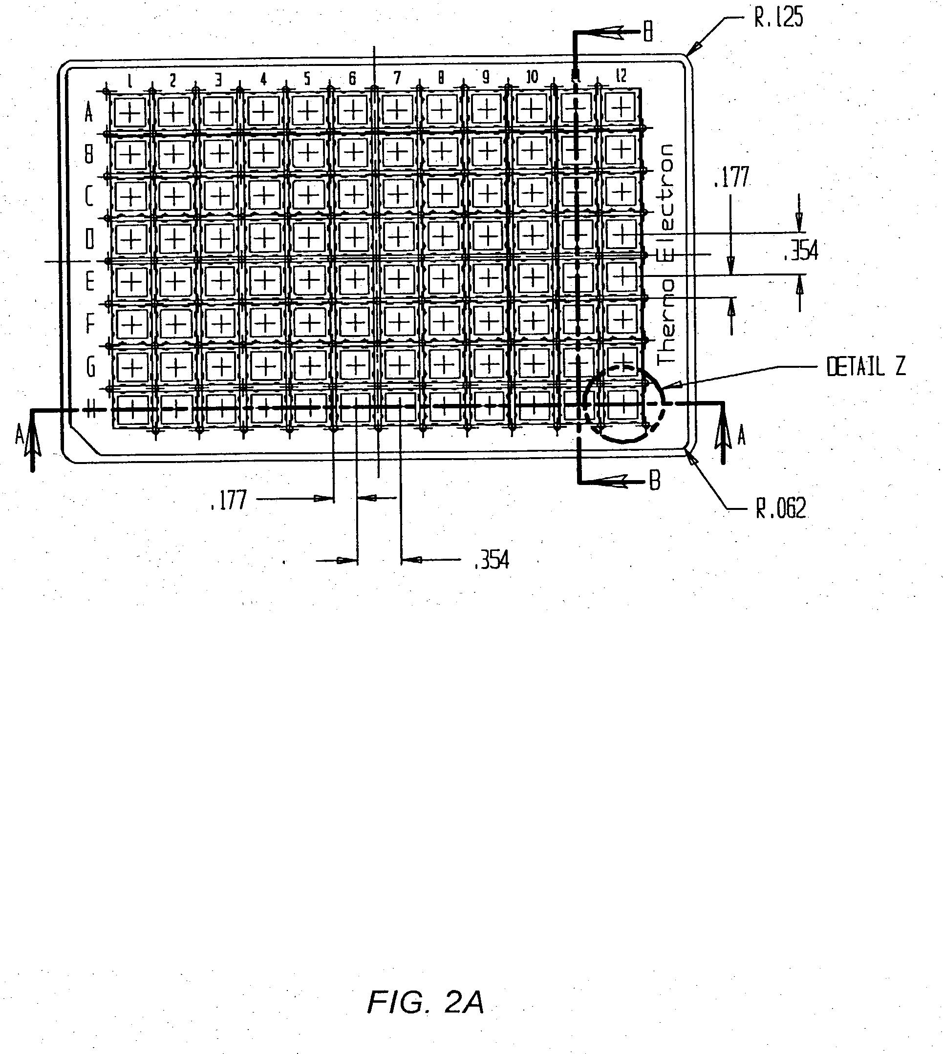
[0192] This study was designed to determine the performance tolerance of the image analysis station to tilt of a sample to be imaged in the x- and y-directions. A test surface with reacted and unreacted zones was placed on a goniometer that was placed in the optical field at the same depth of field, level of focus, and resolution that would be used in analyzing a test surface in a well of the 96 well plate. The goniometer allows very fine adjustments to the angle of tilt applied to the test surface. The test surface was evaluated with tilt applied to the x- and then the y-direction. Readings for a single reacted spot were taken at various angles of positive and negative tilt, as noted in the following table.

7 Contrast Tilt Angle (Positive-Negative) Total I -10 525 811 -5 843 1316 -4 914 1477 -3 920 1484 -2 992 1560 -1 990 1548 0 1014 1496 1 1027 1446 2 1028 1427 3 1007 1361 4 1021 1383 5 1001 1369 6 1008 1363 7 943 1247 8 887 1156 10 795 1058 Data is the same in the x -and y - direc...

example 3

[0194] To establish what if any impact ambient light may have on the measured signal intensity of reacted spots using the image analysis station, a plate containing multiple reacted surfaces was placed in the plate holder of the stage and aligned under the camera for imaging. Signal intensity of the various spots on the reacted test surface were measured in the presence and absence of ambient room light. Three reacted surfaces were measured at a polarizer setting of 45.degree. (midpoint) of dial range and a lamp position that is the dial mark just left of the top position and represents a moderate input intensity. Measurements were made at a number of sample positions on different test surfaces. The correlation of individual spot intensities for all spot positions in well C8 with and without room light is 93.7%. The correlation of individual spot intensities for all spot positions in well E8 with and without room light is 94.6%. Thus ambient light appears to have a minimal impact on...


PUM


Abstract

An image analysis workstation for analyzing optical thin film arrays is disclosed. One disclosed embodiment relates to individual arrays that comprise a single optical thin film test surface that provides a plurality of discretely addressable locations, each comprising an immobilized capture reagent for an analyte of interest. These are referred to herein as "arrayed optical thin film test surfaces." Preferably, an individual arrayed optical thin film test surface comprises at least 4, more preferably at least 16, even more preferably at least 32, still more preferably at least 64, and most preferably 128 or more discretely addressable locations. One or more of the discretely addressable locations may provide control signals (e.g., for normalizing signals and/or that act as positive and/or negative controls) or fiducial signals (i.e., information that is used to determine the relative alignment of the arrayed optical thin film test surface within the device.

Description

[0001] This invention relates to the optical detection, resolution, and identification of an array of elements, preferably for use on an optical thin film surfaceBACKGROUND OF INVENTION[0002] The following description of the background of the invention is provided simply as an aid in understanding the invention and is not admitted to describe or constitute prior art to the invention.[0003] In the semiconductor field, films formed by vacuum evaporation, vapour deposition, spin coating or dip coating are commonly used at various stages of the semiconductor fabrication process. Control and monitoring of the actual thickness and physical properties of thin film layers is absolutely essential to the function of the devices created using this technology. These characteristics must often be monitored during and after fabrication. "Optical thin film determination" refers to methods for determining the thicknesss of one or multiple thin layer(s) formed on a substrate surface. Such "thin film...

Claims


Application Information

Patent Timeline
IPC IPC(8): G01M11/00G01N21/21G01N21/25G01N21/64G01N21/84G06T5/00G06T7/00G06V30/422
CPCG01M11/00G01N21/211G01N21/253G01N21/6452G01N21/6456G01N21/8422G06K9/00G06K2209/19G06T7/0042G06T7/0083G06T2207/20061G06T2207/20132G06T2207/30072G06T2207/30148G06T7/73G06T7/12G06V2201/06G06V30/422G01N33/543G01N21/00G01N33/52G06F18/00
Inventor REA, LARRYCLARK, DAVID D.JENISON, ROBMAUL, DIANA
Owner INVERNESS MEDICAL - BIOSTAR
Why Eureka
Try Eureka