Thin film electrode for forming ohmic contact in light emitting diodes and laser diodes using nickel-based solid solution for manufacturing high performance gallium nitride-based optical devices, and method for fabricating the same

a technology of light-emitting diodes and thin film electrodes, which is applied in the direction of semiconductor lasers, semiconductor/solid-state device details, lasers, etc., can solve the problems of low production efficiency, high manufacturing cost, and inability to develop high-quality ohmic contact systems having a high transmittance in the short-wavelength region

Active Publication Date: 2004-11-11
GWANGJU INST OF SCI & TECH +1
View PDF4 Cites 23 Cited by
  • Summary
  • Abstract
  • Description
  • Claims
  • Application Information

AI Technical Summary

Benefits of technology

[0018] Therefore, the object of the present invention is to provide an ohmic contact metal system with excellent electrical, optical, thermal and structural properties which exhibits an increased effective carrier concentration ({circle over (1)}, {circle over (3)} and {circle over (4)}), a reduced Schottky barrier through a controlled energy bandgap between materials ({circle over (5)}) and a high transmittance ({circle over (2)}).

Problems solved by technology

However, there are some problems in the formation of a high quality ohmic contact using p-type gallium nitride.
Accordingly, the formation of a high quality ohmic contact is difficult.
Moreover, a low carrier (hole) injection makes the manufacture of high grade optical devices difficult.
Another problem is that no high quality ohmic contact systems having a high transmittance in the short-wavelength region have been developed.
The ohmic contact using such a thin metal layer can achieve high transmittance, but it is difficult to obtain a sufficient current injection and spreading capabilities, causing low efficiency of optical devices.
In particular, when annealed at 550.degree. C. for 1 minute, the current-voltage characteristics of the nickel / ruthenium (Ni / Ru) ohmic structure was identified to be difficult structures to form an ohmic contact.

Method used


Image

  • Thin film electrode for forming ohmic contact in light emitting diodes and laser diodes using nickel-based solid solution for manufacturing high performance gallium nitride-based optical devices, and method for fabricating the same
  • Thin film electrode for forming ohmic contact in light emitting diodes and laser diodes using nickel-based solid solution for manufacturing high performance gallium nitride-based optical devices, and method for fabricating the same
  • Thin film electrode for forming ohmic contact in light emitting diodes and laser diodes using nickel-based solid solution for manufacturing high performance gallium nitride-based optical devices, and method for fabricating the same

Examples


example 2

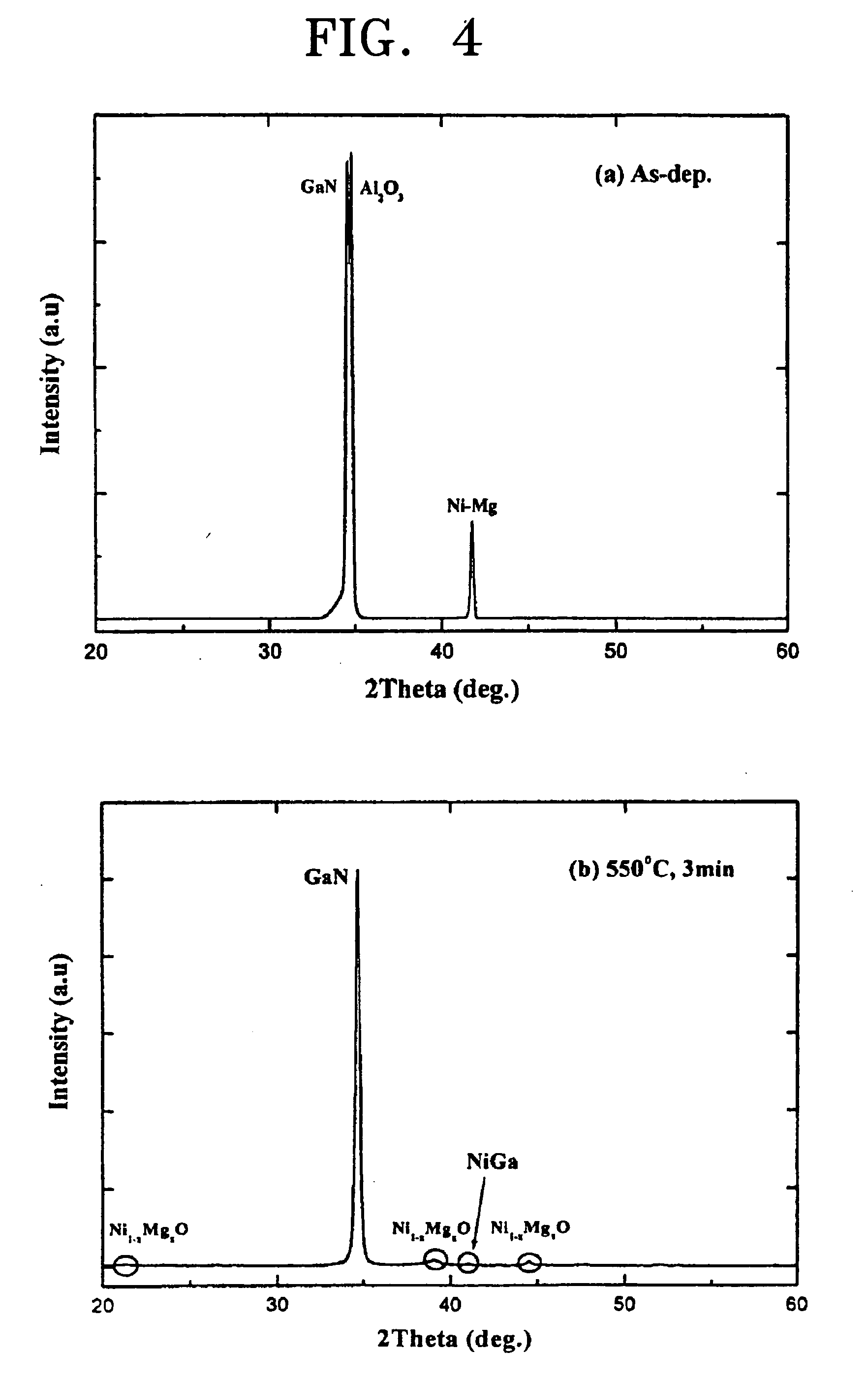
[0098] A procedure was performed in the same manner as in Example 1 up to the step of depositing a Ni--Mg solid solution. Thereafter, platinum (Pt) was deposited using an electron-beam evaporator to form a capping layer in a thickness of 100 .ANG., and then subjected to a lift-off process using acetone. The resulting structure was charged into a rapid thermal annealing (RTA) furnace and annealed in air at 450.about.650.degree. C. for 1 minute to fabricate a thin metal film for forming an ohmic contact.

example 3

[0099] A procedure was performed in the same manner as in Example 1 up to the step of depositing a Ni--Mg solid solution. Thereafter, palladium (Pd) was deposited using an electron-beam evaporator to form a capping layer in a thickness of 100 .ANG., and then subjected to a lift-off process using acetone. The resulting structure was charged into a rapid thermal annealing (RTA) furnace and annealed in air at 450.degree. C. for 1 minute to fabricate a thin metal film for forming an ohmic contact.

example 4

[0100] A procedure was performed in the same manner as in Example 1 up to the step of depositing an electrode layer on a gallium nitride layer. Thereafter, ruthenium (Ru), a nickel-magnesium (Ni--Mg) solid solution and gold (Au) were sequentially deposited in thicknesses of 50 .ANG. and 50 .ANG., respectively, using an electron-beam evaporator and then subjected to a lift-off process using acetone. The resulting structure was charged into a rapid thermal annealing (RTA) furnace and annealed in air at 350.about.650.degree. C. for 1 minute to fabricate a thin metal film for forming an ohmic contact.


PUM

PropertyMeasurementUnit
transmittanceaaaaaaaaaa
thicknessaaaaaaaaaa
carrier concentrationaaaaaaaaaa

Abstract

Disclosed herein is a technique for forming a high quality ohmic contact utilizable in the fabrication of short-wavelength light emitting diodes (LEDs) emitting blue and green visible light and ultraviolet light, and laser diodes (LDs) using a gallium nitride (GaN) semiconductor. The ohmic contact is formed by depositing a nickel (Ni)-based solid solution on top of a p-type gallium nitride semiconductor. The ohmic contact thus formed has an excellent current-voltage characteristic and a low specific contact resistance due to an increased effective carrier concentration around the surface of the gallium nitride layer, as well as a high transmittance in the short-wavelength region.

Description

[0001] This application claims the priority of Korean Patent Application No. 2003-29073, filed on May 7, 2003, in the Korean Intellectual Property Office, the disclosure of which is incorporated herein by reference in its entity.[0002] The present invention relates to a technique for forming a high quality ohmic contact with improved current injection and spreading capabilities, as well as low ohmic contact resistance and high transmittance. The technique for forming a high quality ohmic contact is one of the key techniques for the fabrication of short-wavelength light emitting diodes (LEbs) emitting blue and green visible light and ultraviolet light, and laser diodes (LDs) using a gallium nitride (GaN) semiconductor.DESCRIPTION OF THE RELATED ART[0003] The formation of a high quality ohmic contact between a semiconductor and an electrode is very important to manufacture photo-related devices using a gallium nitride semiconductor such as light emitting diodes and laser diodes.[0004]...

Claims


Application Information

Patent Timeline
Patent Type & Authority Applications(United States)
IPC IPC(8): H01L21/28H01L21/285H01L33/30H01L33/32H01L33/40H01S5/042H01S5/30H01S5/323
CPCH01L21/28575H01L33/32H01L33/40H01S5/0421H01S5/0425H01S5/3054H01S5/32341H01S5/0014H01S5/04253
Inventor SONG, JUNE-OLEEM, DONG-SUKSEONG, TAE-YEON
Owner GWANGJU INST OF SCI & TECH
Why Eureka
Try Eureka