
GaN-based high-electron-mobility transistor epitaxial wafer and preparation method thereof

A high electron mobility, gallium nitride-based technology, applied in the field of gallium nitride-based high electron mobility transistor epitaxial wafer and its preparation, can solve the problems of high activation energy, high doping concentration, low ionization rate and the like

Active Publication Date: 2021-01-12
HC SEMITEK ZHEJIANG CO LTD
View PDF5 Cites 3 Cited by
  • Summary
  • Abstract
  • Description
  • Claims
  • Application Information

AI Technical Summary

Problems solved by technology

[0004] At present, the P-type GaN cap layer is mainly doped with Mg, but Mg doped has the problem that it is easily passivated by H, resulting in high activation energy, and the ionization of Mg The rate is very low, and a higher doping concentration is required to achieve P-type, and Mg as an acceptor will also form a complex with N vacancies in GaN MgGa-VN, forming a self-compensation effect, resulting in a decrease in the carrier concentration

Method used


Image

  • GaN-based high-electron-mobility transistor epitaxial wafer and preparation method thereof
  • GaN-based high-electron-mobility transistor epitaxial wafer and preparation method thereof
  • GaN-based high-electron-mobility transistor epitaxial wafer and preparation method thereof

Examples


Embodiment Construction

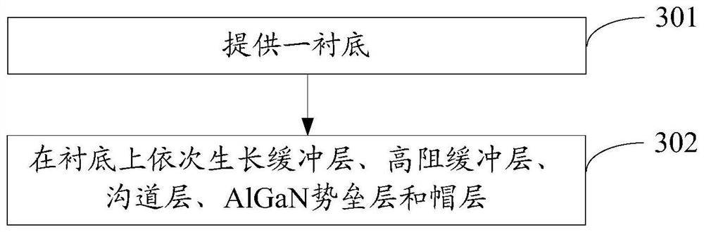
[0028] In order to make the purpose, technical solution and advantages of the present disclosure clearer, the implementation manners of the present disclosure will be further described in detail below in conjunction with the accompanying drawings.

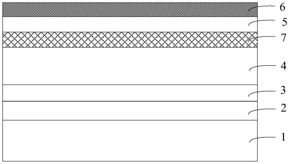
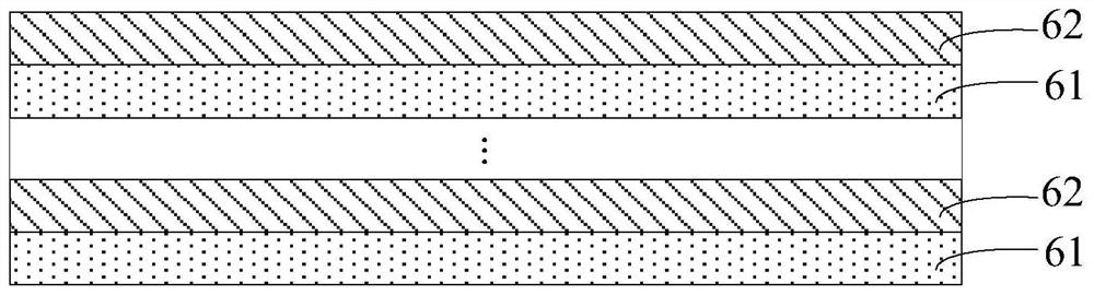
[0029] GaN-based power electronic devices have attracted a lot of attention in recent years. GaN materials can form heterojunction structures with AlGaN, InGaN and other materials. Due to the spontaneous polarization and piezoelectric polarization effects of the barrier layer materials, a high concentration of two-dimensional electron gas (2DEG) will be formed at the heterojunction interface. Due to the advantages of GaN materials such as large band gap, high electron mobility, high electron saturation velocity and large breakdown field strength, gallium nitride-based HEMT (High Electron Mobility Transistor, high electron mobility transistor) has become a Research hotspots in the field of microwave power and circuits.

[0030] Al...


PUM

PropertyMeasurementUnit
Doping concentrationaaaaaaaaaa

Abstract

The invention provides a GaN-based high-electron-mobility transistor epitaxial wafer and a preparation method thereof, and belongs to the technical field of semiconductors. The GaN-based high-electron-mobility transistor epitaxial wafer comprises a substrate, a buffer layer, a high-resistance buffer layer, a channel layer, an AlGaN barrier layer and a cap layer, wherein the buffer layer, the high-resistance buffer layer, the channel layer, the AlGaN barrier layer and the cap layer are stacked on the substrate, the cap layer comprises first sub-layers and second sub-layers which grow alternately, the first sub-layers are GaN layers, and the second sub-layers are InGaN layers. The first sub-layer and the second sub-layer are both doped with a main doping element, the main doping element is Be or Mg, the second sub-layer is also doped with an auxiliary doping element, and the auxiliary doping element is O, Mg, Si or Zn. According to the GaN-based high-electron-mobility transistor epitaxial wafer, the generation of complexes can be reduced, and the activation energy of the P-type dopant in the cap layer is reduced, so that the P-type cap layer with high doping concentration is obtained.

Description

technical field [0001] The disclosure relates to the technical field of semiconductors, in particular to a gallium nitride-based high electron mobility transistor epitaxial wafer and a preparation method thereof. Background technique [0002] HEMT (High Electron Mobility Transistor, High Electron Mobility Transistor) based on AlGaN (aluminum gallium nitride) / GaN (gallium nitride) heterostructure has high current density, critical breakdown voltage and electron mobility. The field of high temperature electronic devices has very important application value. [0003] A HEMT typically includes a chip and a source, drain, and gate located on the chip. Chips are obtained from epitaxial wafers. The structure of the epitaxial wafer generally includes a substrate and a buffer layer, a high-resistance buffer layer, a channel layer, an AlGaN barrier layer and a cap layer sequentially stacked on the substrate. At present, there are four main technologies in the world to realize galli...

Claims


Application Information

Patent Timeline
IPC IPC(8): H01L29/778H01L29/36H01L21/335
CPCH01L29/7786H01L29/36H01L29/66462Y02P70/50H01L29/2003H01L29/207H01L29/155H01L29/157H01L21/02507H01L21/02505H01L21/0254H01L21/02458H01L21/0262H01L21/02579
Inventor 苏晨胡加辉王慧蒋媛媛张武斌李鹏
Owner HC SEMITEK ZHEJIANG CO LTD
Learn More