
Method for increasing doping concentration of phosphor in nanometer silicon material through employing boron-phosphor codoping

A technology of doping concentration and nano-silicon, which is applied in the direction of nanotechnology, nanotechnology, nanotechnology, etc. for materials and surface science, can solve the problems such as difficult impurity doping and doping concentration, and achieve high doping concentration and convenient Accurate direct doping situation, beneficial to the application of technology and the effect of industrialization

Inactive Publication Date: 2017-02-08
NANJING UNIV
View PDF3 Cites 2 Cited by
  • Summary
  • Abstract
  • Description
  • Claims
  • Application Information

AI Technical Summary

Problems solved by technology

[0008] The purpose of the invention is to solve key and difficult problems such as difficult doping of impurities caused by the "self-cleaning" effect and surface defect states in nano-silicon materials and low doping concentration; The method of doping concentration, especially to increase the effective doping concentration of impurities in low-dimensional semiconductor materials, to achieve effective and controllable doping, to solve problems such as impurity distribution and relative energy level position in nano-silicon materials

Method used


Image

  • Method for increasing doping concentration of phosphor in nanometer silicon material through employing boron-phosphor codoping
  • Method for increasing doping concentration of phosphor in nanometer silicon material through employing boron-phosphor codoping
  • Method for increasing doping concentration of phosphor in nanometer silicon material through employing boron-phosphor codoping

Examples


Embodiment Construction

[0029] 1) Prepare a boron-phosphorus co-doped nano-silicon / silicon dioxide multilayer film on a silicon substrate;

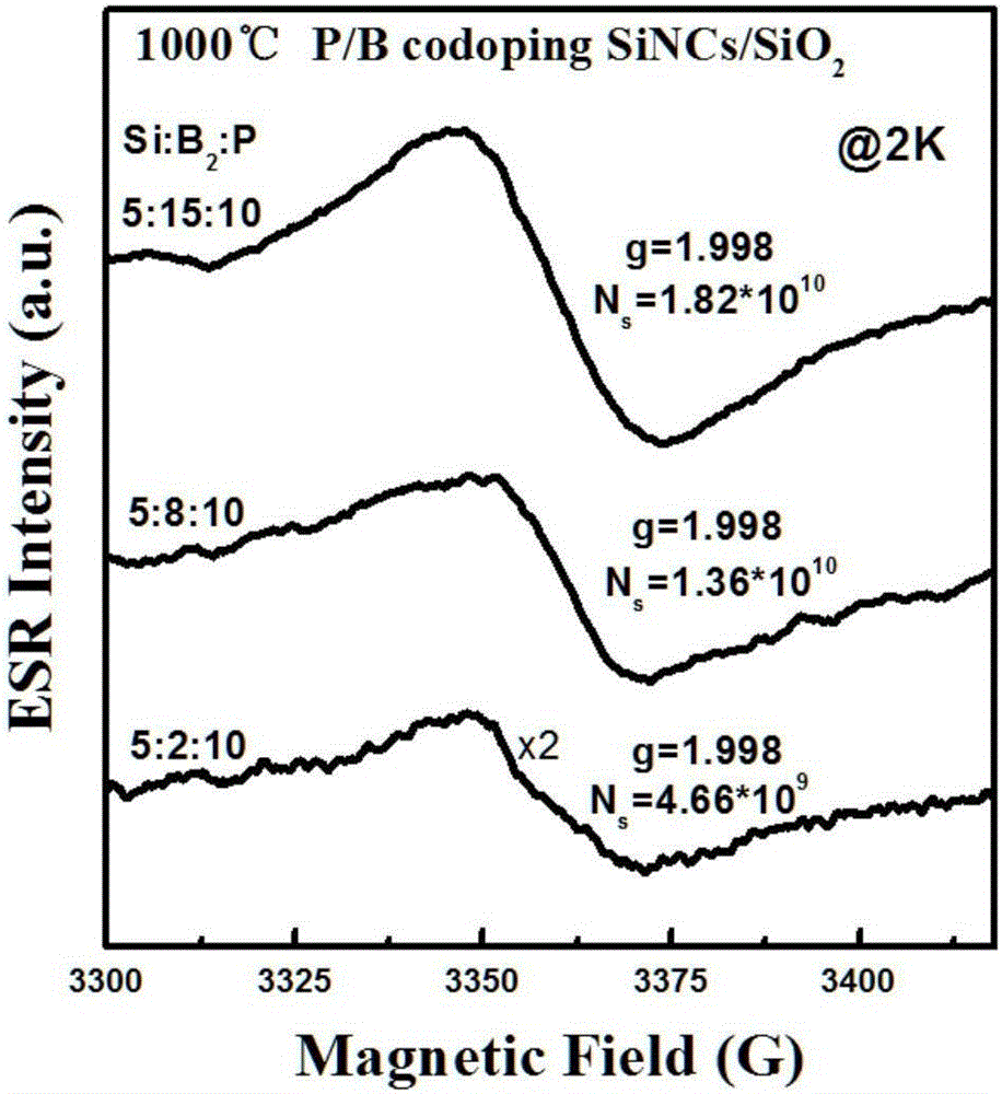
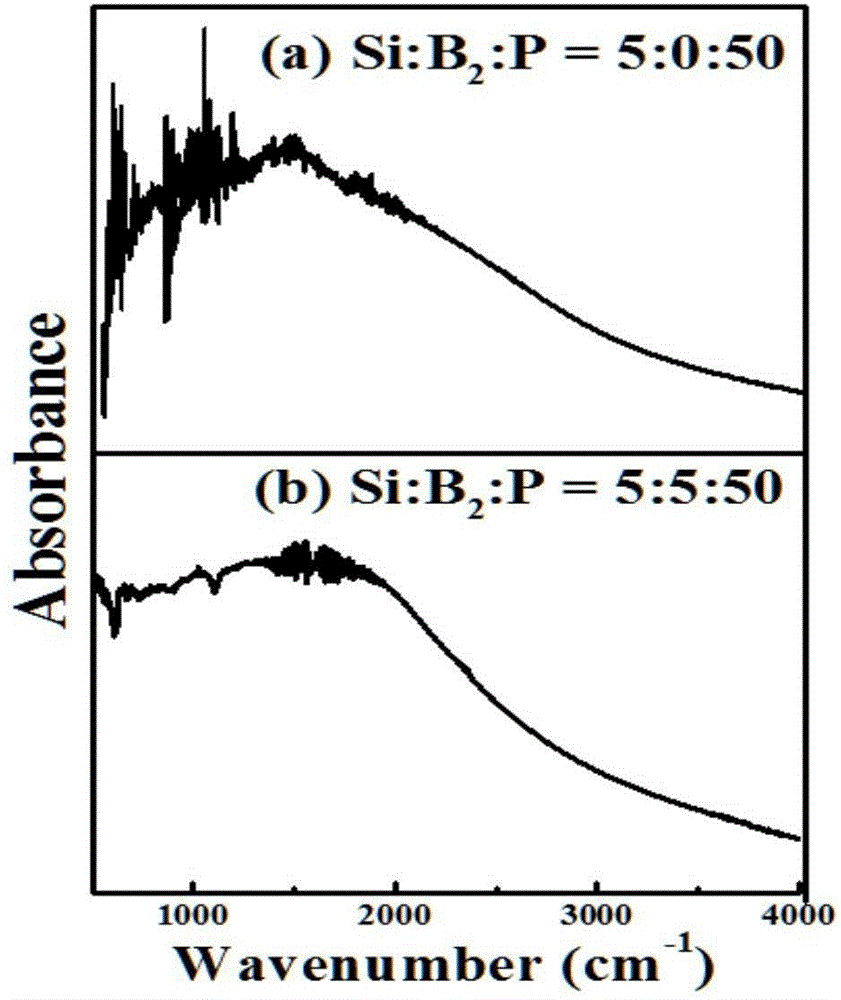
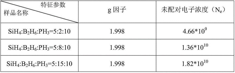
[0030] Using the RCA standard cleaning process, the cleaned p-type single crystal silicon substrate (resistivity: 1.5-3Ω·cm) and quartz substrate were placed in a PECVD system for film deposition, and argon (Ar ) to pretreat the cleaned substrate surface, the power is 30W, the reaction pressure is 480mTorr, the time is 5min, and then the argon gas is turned off, oxygen gas is introduced, and oxidation treatment is carried out for 90s. The purpose of pretreatment is to strengthen the adhesion between the film and the substrate. During film growth, silane (SiH 4 ) to deposit an amorphous silicon layer, the silane flow control is 5 sccm, and the reaction time is 90s, during which 1% vol phosphine diluted with hydrogen gas and 1 vol% borane diluted with hydrogen gas are fed to realize co-doping of boron and phosphorus, changing phosphine, The borane flow rate can ob...


PUM

PropertyMeasurementUnit
electrical resistivityaaaaaaaaaa

Abstract

The invention discloses a method for increasing the doping concentration of phosphor in a nanometer silicon material through employing the boron-phosphor codoping technology, and the method comprises the following steps: 1), preparing a multilayer film material doped with nanometer silicon / silicon oxide through employing PECVD; 2), obtaining the multilayer film material doped with nanometer silicon / silicon oxide (a-Si / SiO2) through the alternate conducting of two processes: noncrystalline silicon layer deposition / in-situ oxidation, and obtaining the thickness of the a-Si / SiO2 multilayer film through controlling the time of the noncrystalline silicon layer deposition / in-situ oxidation; 3), carrying out the dehydrogenation processing of the prepared a-Si / SiO2 multilayer film; 4), carrying out the high-temperature annealing under the nitrogen condition after dehydrogenation, enabling polycrystalline silicon to be crystalized to form nanometer silicon, activating foreign matter atoms to enter the nanometer silicon, and achieving the doping of the nanometer silicon. The method prepares the codoping nanometer silicon / silicon oxide multilayer film.

Description

[0001] 1. Technical field [0002] The present invention proposes a method that can solve the difficulty of doping nanomaterials and increase the doping concentration of impurities in nano-silicon, especially a new method that can increase the effective doping concentration of phosphorus in nano-silicon-based thin films through boron-phosphorus co-doping technology. technology. [0003] 2. Background technology [0004] Silicon (Si) is currently the most important semiconductor material. Since the 1960s, silicon materials have been widely used in microelectronics, solar photovoltaics, semiconductor integrated circuits and other fields. The development of the semiconductor industry based on silicon materials has greatly promoted the development of electronic science and information technology. With the development of semiconductor technology and devices, the size of silicon materials used in devices is also decreasing, and has entered the deep submicron and even nanoscale so fa...

Claims


Application Information

Patent Timeline
Patent Type & Authority Applications(China)
IPC IPC(8): H01L21/02B82Y30/00
CPCH01L21/02164H01L21/02274H01L21/02381H01L21/02532H01L21/0257H01L21/02592H01L21/0262H01L21/02667B82Y30/00
Inventor 徐骏李东珂陆鹏李伟翟颖颖陈坤基
Owner NANJING UNIV
Learn More