Reactor for producing reactive intermediates for low dielectric constant polymer thin films

a polymer thin film, reactive intermediate technology, applied in indirect heat exchangers, semiconductor/solid-state device details, lighting and heating apparatus, etc., can solve the problems of inconvenient production of dimers via solvent trapping method, and inability to meet the requirements of sub-90 micron integrated circuits

Inactive Publication Date: 2005-01-06
DIELECTRIC SYST INT
View PDF53 Cites 17 Cited by
  • Summary
  • Abstract
  • Description
  • Claims
  • Application Information

AI Technical Summary

Benefits of technology

A reactor for forming a reactive intermediate from a precursor for the deposition of a low dielectric constant polymer film via transport polymerization is disclosed. The reactor includes an inlet for admitting a flow of the precursor into the reactor, an interior

Problems solved by technology

However, the dielectric constants and dimensional/thermal stability of PPX and PPX-D are unsuitable for use in sub-90 micron integrated circuits.
However, the generation of a sufficient enough quantity of highly pure *CF2—C6H4—CF2* diradicals for the commercial use of PPX-F in integrated circuits has posed many problems, as it is difficult to synthesize the dimer (CF2—C6H4—CF2)2 in sufficient quantities for commercial applications.
However, the solvent-trapped dimer is not in a useful state for commercial scale integrated circuit production.
Furthermore, production of the dimer via this method may be prohibitively expensive.
However, the “catalysts” would actually serve as reactants in this process for the formation of metal bromides, thus clogging the reactor and preventing further debromination.
Also, the particular metal bromides formed may migrate to deposition chamber and contaminate the wafer and may be difficult to reduce back to elemental metals.
Another

Method used


Image

  • Reactor for producing reactive intermediates for low dielectric constant polymer thin films
  • Reactor for producing reactive intermediates for low dielectric constant polymer thin films
  • Reactor for producing reactive intermediates for low dielectric constant polymer thin films

Examples


Embodiment Construction

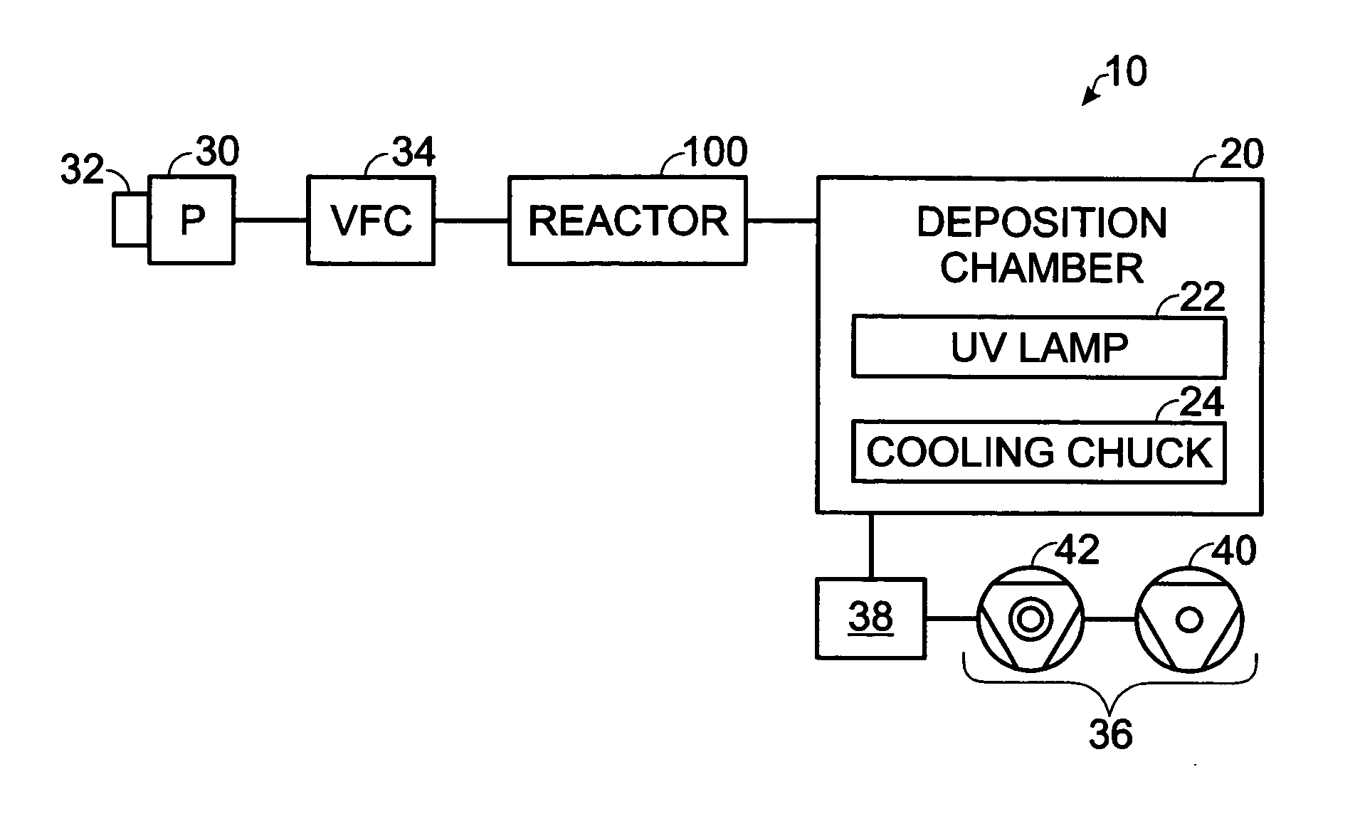
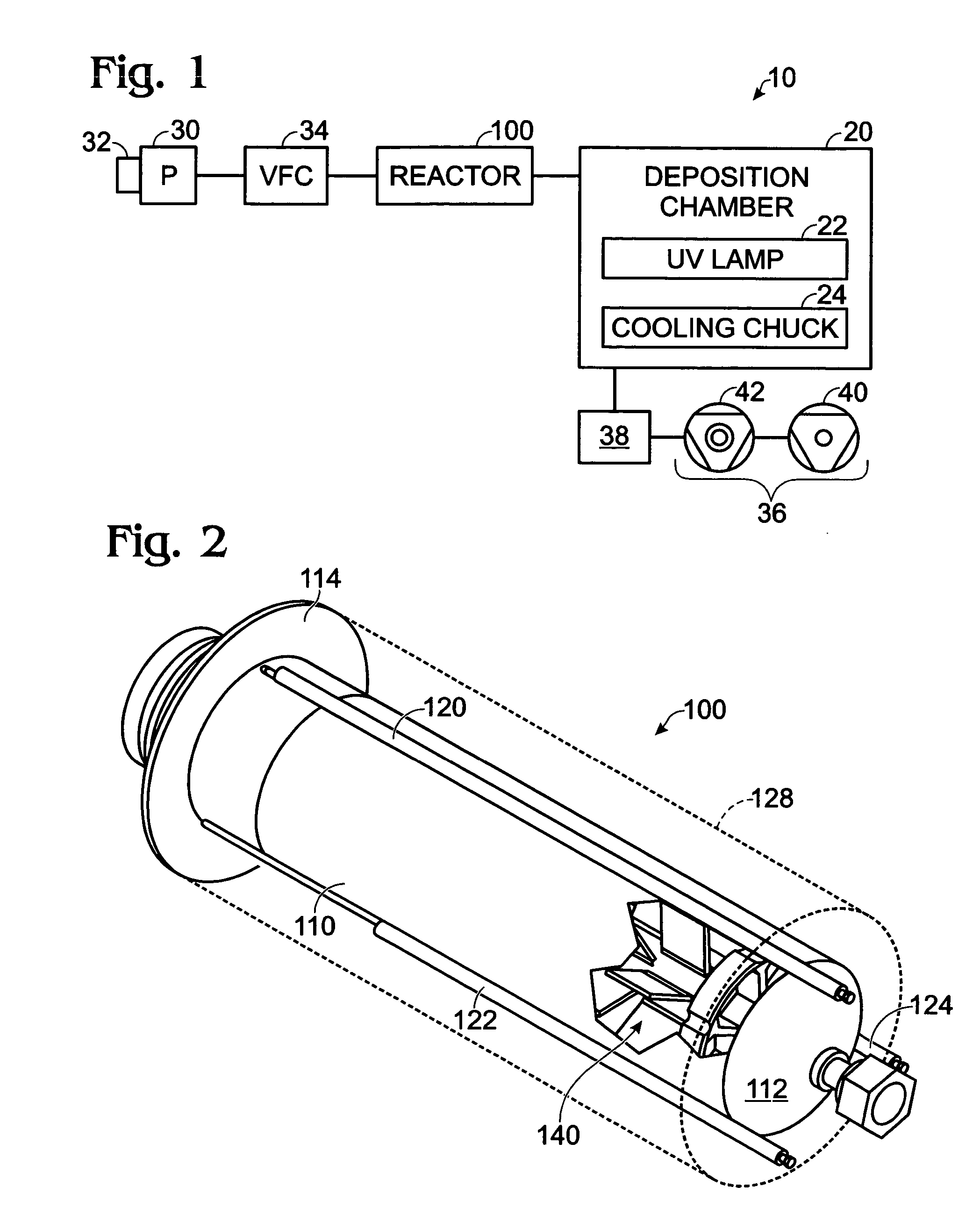
FIG. 1 shows, generally at 10, a vapor deposition system for depositing a polymer dielectric film on a wafer via transport polymerization. System 10 is at times described herein in the context of a system for depositing a PPX-F film, but it will be appreciated that the concepts set forth herein may be extended to any other suitable low dielectric constant polymer film deposition system.

Vapor deposition system 10 includes a vapor deposition chamber 20, and a wafer holder 22 for holding a wafer during deposition. Deposition chamber 20 may also include an energy source, such as an ultraviolet light source 24, for various purposes, for example, for drying a wafer surface before depositing a low dielectric constant film, or for activating the polymerization of a keto-, vinyl- or halo-organosilane layer that may be deposited above or below the low dielectric constant polymer film. Exemplary organosilane materials and uses thereof are disclosed in U.S. patent application Ser. No. 10 / 816,2...


PUM

PropertyMeasurementUnit
Flow rateaaaaaaaaaa
Transparencyaaaaaaaaaa
Energyaaaaaaaaaa

Abstract

A reactor for forming a reactive intermediate from a precursor for the deposition of a low dielectric constant polymer film via transport polymerization is disclosed. The reactor includes an inlet for admitting a flow of the precursor into the reactor, an interior for converting the precursor to the reactive intermediate, an outlet for admitting a flow of the reactive intermediate out of the interior, and at least one of an energy source and an oxidant source associated with the outlet for decomposing residues in the outlet.

Description

BACKGROUND Integrated circuits contain many different layers of materials, including dielectric layers that insulate adjacent conducting layers from one another. With each decrease in the size of integrated circuits, the individual conducting layers and elements within the integrated circuits grow closer to adjacent conducting elements. This necessitates the use of dielectric layers made of materials with low dielectric constants to prevent problems with capacitance, cross talk, etc. between adjacent conducting layers and elements. Low dielectric constant polymers have shown promise for use as dielectric materials in integrated circuits. Examples of low dielectric constant polymers include, but are not limited to, fluoropolymers such as TEFLON ((—CF2—CF2—)n; kd=1.9) and poly(paraxylylene)-based materials such as PPX-F ((—CF2—C6H4—CF2—)n; kd=2.23). Many of these materials have been found to be dimensionally and chemically stable under temperatures and processing conditions used in ...

Claims


Application Information

Patent Timeline
IPC IPC(8): B01J19/12B01J19/18B05D1/00B05D3/02B05D3/06B05D7/24B29C71/02C08G61/02C08J5/18C08L65/00C08L65/04C23C16/452F28D17/00H01L21/312H01L21/768H01L23/532
CPCB01J19/123H01L2924/09701B01J2219/00153B01J2219/00159B01J2219/0879B05D1/007B05D1/60B05D3/0254B05D3/061B05D3/062B29C71/02B29C2071/022B29C2071/025B29C2071/027C08G61/02C08G61/025C08G2261/3424C08J5/18C08J2365/04C08L65/00C08L65/04C23C16/452F28D17/005H01L21/0212H01L21/02263H01L21/312H01L21/3127H01L23/53238H01L23/5329B01J19/1887H01L2924/0002H01L2924/00
Inventor LEE, CHUNG J.KUMAR, ATULCHEN, CHIEH
Owner DIELECTRIC SYST INT
Why Eureka
Try Eureka