
Methods and systems for inspection of wafers and reticles using designer intent data

a technology of designer intent and inspection method, applied in the direction of semiconductor/solid-state device testing/measurement, image enhancement, instruments, etc., can solve the problems of random defects, defects such as film thickness variation or lateral dimension variation, and particulate contamination and pattern defects being introduced into semiconductor devices

Active Publication Date: 2005-01-06
KLA TENCOR TECH CORP
View PDF24 Cites 194 Cited by
  • Summary
  • Abstract
  • Description
  • Claims
  • Application Information

AI Technical Summary

Benefits of technology

[0029] In another embodiment, the method may include determining an overall significance of different regions on the reticle. In one such embodiment, the method may include determining one or more parameters of a process used to fabricate the different regions of the reticle based on the overall significance of the different regions. In a different such embodiment, the method may include altering one or more parameters of a process used to inspect the different regions of the reticle based on the overall significance of the different regions. In yet another such embodiment, the method may include altering one or more parameters of a process used to repair the reticle based on the overall significance of the different regions. In this manner, a process used to fabricate, inspect, or repair a reticle may have one or more parameters in one of the different regions that are different than the one or more parameters of the process in another of the different regions.
[0030] In some embodiments, the method may include determining one or more parameters of a process that is used to repair the defect based on the overall significance of the defect. The one or more parameters used to repair different defects on the reticle may be different. In another embodiment, the method may include determining processing of the reticle based on the overall significance of the defect. The processing may include rejecting the reticle, repairing the reticle, or cleaning the reticle.
[0031] In an additional embodiment, the method may include generating a visual representation

Problems solved by technology

During each semiconductor fabrication process, defects such as particulate contamination and pattern defects may be introduced into semiconductor devices.
For example, random defects may be caused by events such as an unexpected increase in particulate contamination in a manufacturing environment and an unexpected increase in contamination in process chemicals that may be used in fabrication of a semiconductor device.
Defects caused by individual process marginalities or by interactions between multiple processes may result in defects such as a film thickness variation or a lateral dimension variation due to dose variation.
Such defects may, in turn, result in a defect in a semiconductor device formed on the specimen such as bridging between two conductive structures thereby forming a short between the structures.
Defects repeated within each semiconductor device formed on an entire specimen may, for example, be systematically caused by contamination or defects found on a reticle, or a mask.
As the dimensions of advanced semiconductor devices continue to shrink, the presence of defects in the semiconductor devices limits the successful fabrication, or yield, of a semiconductor device.
For example, a reticle defect reproduced in a resist patterned during lithography may cause an open circuit or a short circuit in a semiconductor device formed in subsequent processing.
Because fabrication of a semiconductor device includes many complex process steps, the adverse effects of defects on total yield may increase exponentially if an error that is caused by a defect is propagated throughout an entire manufacturing process or operation over time.

Method used


Image

  • Methods and systems for inspection of wafers and reticles using designer intent data
  • Methods and systems for inspection of wafers and reticles using designer intent data
  • Methods and systems for inspection of wafers and reticles using designer intent data

Examples


Embodiment Construction

[0046] The term “wafer” generally refers to substrates formed of a semiconductor or non-semiconductor material. Examples of such a semiconductor or non-semiconductor material include, but are not limited to, monocrystalline silicon, gallium arsenide, and indium phosphide. Such substrates may be commonly found and / or processed in semiconductor fabrication facilities.

[0047] A wafer may include only the substrate such as a virgin wafer. Alternatively, a wafer may include one or more layers that may be formed upon a substrate. For example, such layers may include, but are not limited to, a resist, a dielectric material, and a conductive material. A resist may include a resist that may be patterned by an optical lithography technique, an e-beam lithography technique, or an X-ray lithography technique. Examples of a dielectric material may include, but are not limited to, silicon dioxide, silicon nitride, silicon oxynitride, and titanium nitride. Additional examples of a dielectric mater...


PUM


Abstract

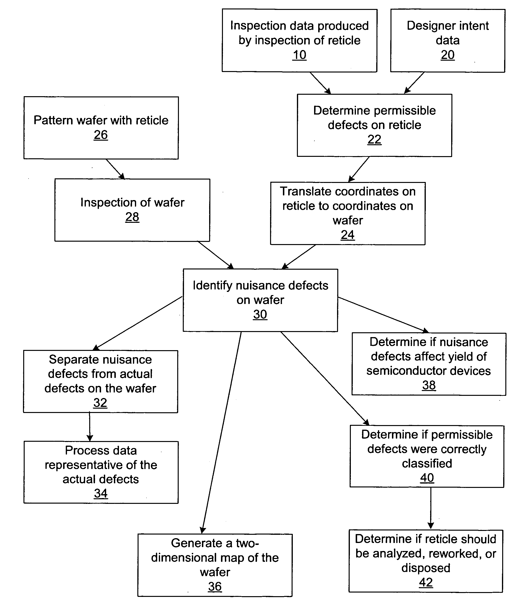
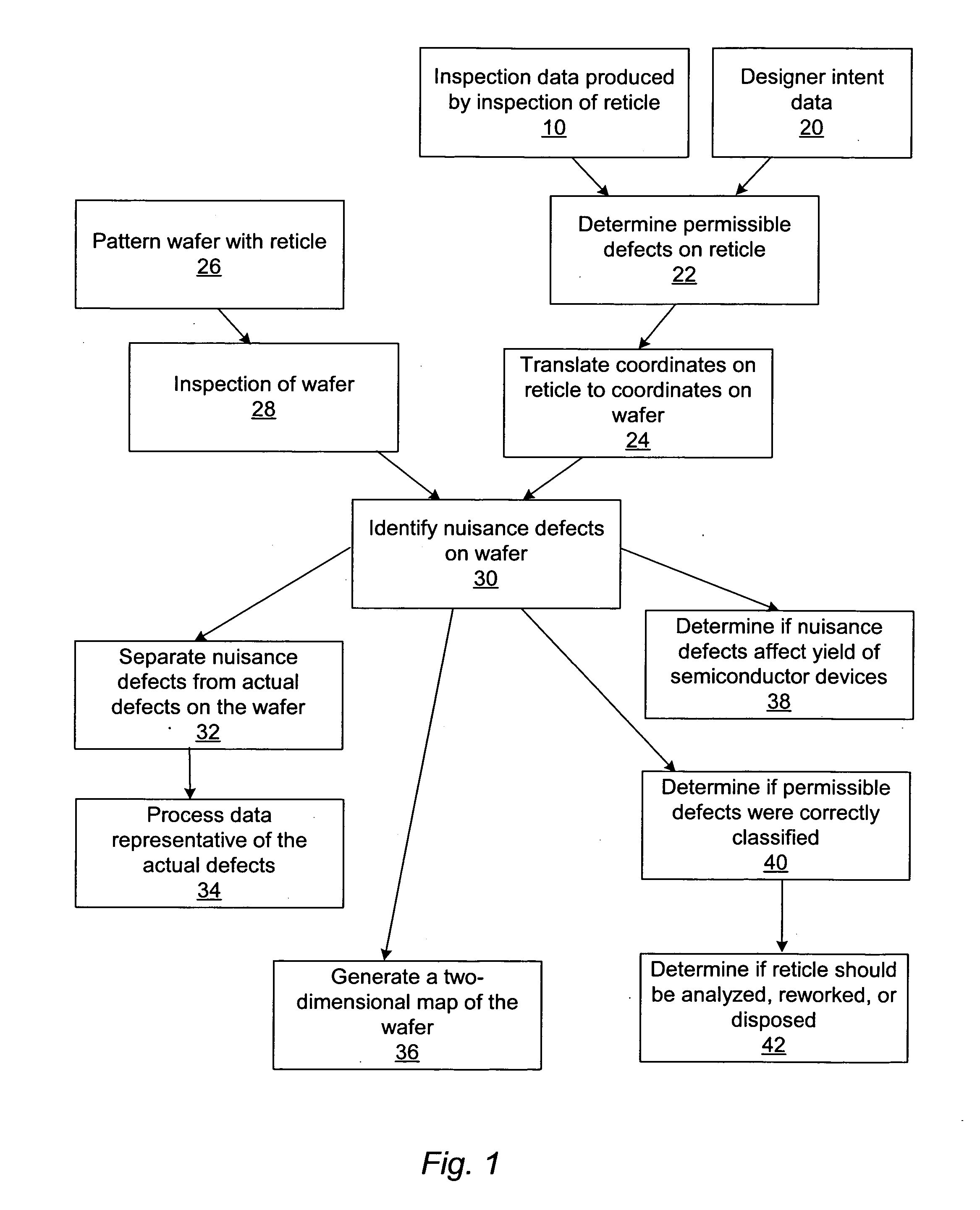
Methods and systems for inspection of wafers and reticles using designer intent data are provided. One computer-implemented method includes identifying nuisance defects on a wafer based on inspection data produced by inspection of a reticle, which is used to form a pattern on the wafer prior to inspection of the wafer. Another computer-implemented method includes detecting defects on a wafer by analyzing data generated by inspection of the wafer in combination with data representative of a reticle, which includes designations identifying different types of portions of the reticle. An additional computer-implemented method includes determining a property of a manufacturing process used to process a wafer based on defects that alter a characteristic of a device formed on the wafer. Further computer-implemented methods include altering or simulating one or more characteristics of a design of an integrated circuit based on data generated by inspection of a wafer.

Description

PRIORITY CLAIM [0001] This application claims priority to U.S. Provisional Application No. 60 / 485,338 entitled “Methods and Systems for Inspection of Wafers and Reticles Using Designer Intent Data,” filed Jul. 3, 2003, which is incorporated by reference as if fully set forth herein.BACKGROUND OF THE INVENTION [0002] 1. Field of the Invention [0003] The present invention generally relates to methods and systems for inspection of wafers and reticles using designer intent data. Certain embodiments relate to systems and methods for detecting defects on a wafer based on data representative of a reticle or data produced by inspection of a reticle. [0004] 2. Description of the Related Art [0005] Fabricating semiconductor devices such as logic and memory devices typically includes processing a specimen such as a semiconductor wafer using a number of semiconductor fabrication processes to form various features and multiple levels of the semiconductor devices. For example, lithography is a se...

Claims


Application Information

Patent Timeline
IPC IPC(8): G01N21/95G03F1/44G03F7/20
CPCG01N21/9501G01N21/956G03F7/7065G03F1/84G01N2021/95676G03F7/20G06T2207/30148G06T7/0006G06T7/0008H01L22/12
Inventor VOLK, WILLIAMWILEY, JAMESWATSON, STERLINGKEKARE, SAGAR A.HESS, CARLMARELLA, PAUL FRANKMCCAULEY, SHARONCHANG, ELLIS
Owner KLA TENCOR TECH CORP
Learn More