Semiconductor memory

a technology of semiconductors and memory, applied in the field of semiconductor memory, can solve the problems of insufficient reduction, insufficient scalability, and difficulty in securing the isolation of the programming threshold voltage and the erasure threshold voltag

Inactive Publication Date: 2005-01-13
KK TOSHIBA
View PDF11 Cites 208 Cited by
  • Summary
  • Abstract
  • Description
  • Claims
  • Application Information

AI Technical Summary

Benefits of technology

An aspect of the present invention inheres in a semiconductor memory with an electrically writable/erasable memory cell having a gate insulating layer including: (a) a first gate insulating layer, which is made from a compound containing at least silicon and oxygen; (b) a first charge storage layer, which is being in contact with the first gate insulating layer, and is made from a silicon nitride film, a silicon oxynitride film, or an alumina film; (c) a second insulating layer, which is thicker than the first gate insulting layer; (d) a second charge storage layer, which is being in contact with the second insulating layer; (e) a third insulating layer, which is being in contact with the second charge storage layer, and is thicker than the first gate insulating layer; and (f) a control electrode, which is formed upon the third insulating layer.
Another aspect of the present invention inheres in a semiconductor memory with an electrically writable/erasable memory cell having a gate insulating layer including: (a) a first gate insulating layer, which is made from a compound containing at least silicon and oxygen; (b) a first charge storage layer, which is being in contact with the first gate insulating layer, and is made from a silicon nitride film, a silicon oxynitride film, or an alumina film; (c) a second insulating layer ha

Problems solved by technology

Accordingly, since a large erasure voltage increases the quantity of the injected electrons in the control electrode to be almost equivalent to the quantity of the injected holes, there was a problem where the erasure threshold voltage would not become lower than a specific value, that is, would not sufficiently decrease.
Therefore, there was a difficult problem of sufficiently securing isolation of the programming threshold voltage and the erasure threshold voltage.
In addition, in the case of injecting holes using the current passing through the first silicon oxide film as the tunneling current, there was a problem where, due to an increase in the quantity of the injected electrons that pass through the second silicon oxide film, the increase in the quantity of the positive charges in the charge

Method used


Image

  • Semiconductor memory
  • Semiconductor memory
  • Semiconductor memory

Examples


first embodiment

(First Embodiment)

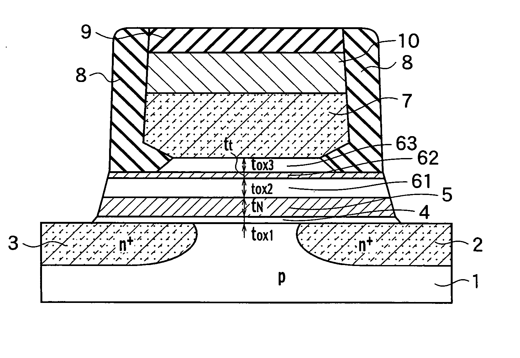
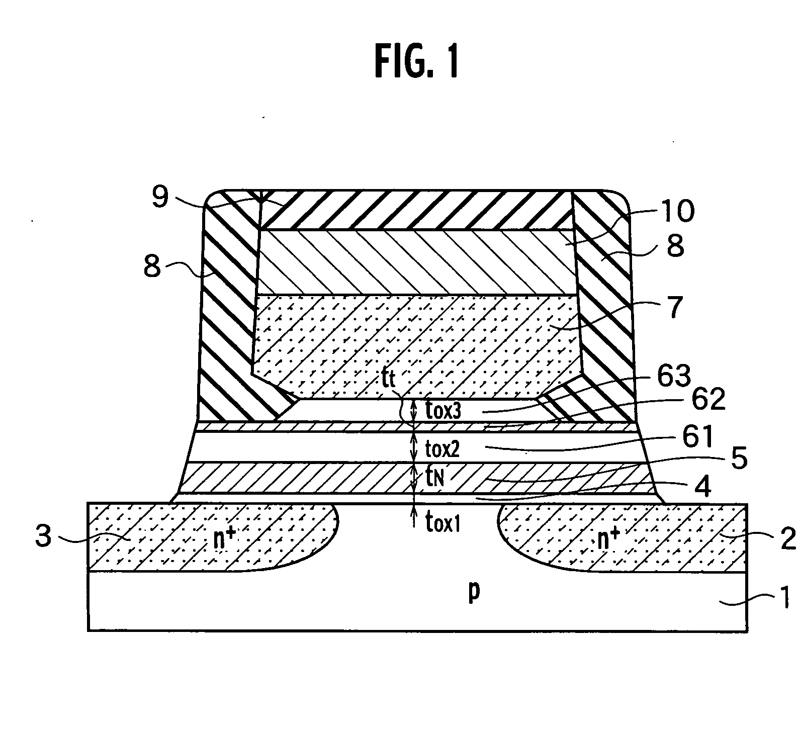
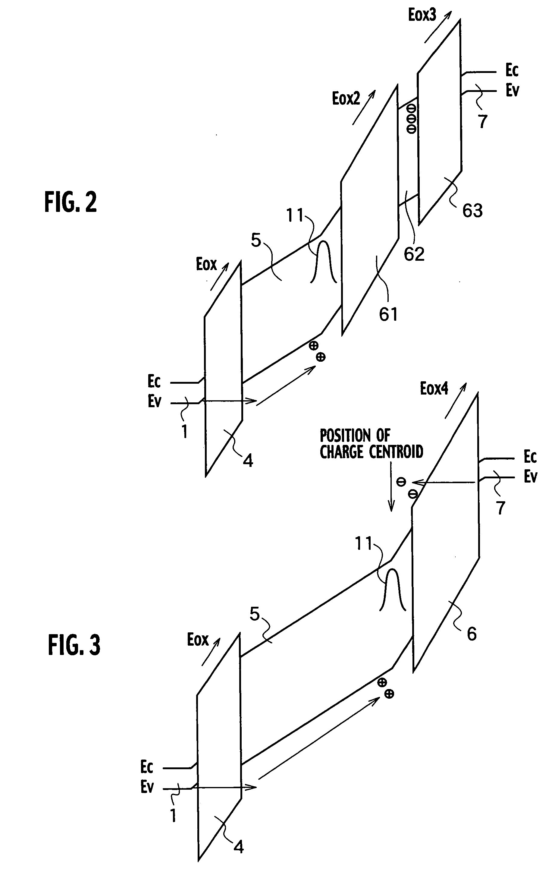
FIG. 1 shows an exemplary structure of a semiconductor memory according to the first embodiment of the present invention. The structure of this embodiment has a feature that, in comparison with a conventional example, has a second charge storage layer 62, for storing negative charges injected from a gate and is arranged in a portion of a second insulating layer corresponding to reference numeral 6 in FIG. 3. In FIG. 1, a first gate insulating layer 4, which is, for example, made from a silicon oxide film or an oxynitride film having a thickness of 0.5 nm to 10 nm, is formed on a p-type silicon semiconductor region 1 where the boron or indium impurity concentration is between 1014 cm−3 and 1019 cm−3, for example. In this case, tox1 denotes the thickness of the flat portion of the first gate insulating layer 4, and εox1 denotes a dielectric constant of the first gate insulating film. In addition, a first charge storage layer 5 having a thickness of 3 nm to 20 nm, whi...

second embodiment

(Second Embodiment)

As shown in FIG. 8, a semiconductor memory according to the second embodiment of the present invention, a control line, which is connected to a control electrode 7, is formed in the same direction as a source region 2, a p-type silicon semiconductor region 1, and a drain region 3 are formed relative to the first embodiment. It should be noted that detailed description for the same configurations as with the first embodiment using the same reference numerals is omitted.

The semiconductor memory according to the second embodiment of the present invention differs from the first embodiment in that a device isolating and insulating layer 12, made from a silicon oxide film, for example, is formed in a self-aligned manner on the source region 2 and the drain region 3. The second embodiment has a feature that, in comparison with the conventional example, a second charge storage layer 62, for storing negative charges injected from a gate and is arranged in a portion of t...

third embodiment

(Third Embodiment)

FIG. 11 shows an exemplary cross sectional structure of a semiconductor memory according to the third embodiment of the present invention. It should be noted that detailed description for the same portions as with the first embodiment and second embodiment using the same reference numerals is omitted.

The semiconductor memory according to the third embodiment of the present invention replaces an insulating layer doped with an accepter impurity for a second charge storage layer 62. The semiconductor memory according to the third embodiment of the present invention has a feature that, in comparison with the conventional example, has a second charge storage layer 62a for storing negative charges by doping the portion corresponding to the second charge storage layer 62 with an acceptor impurity. In FIG. 11, a first gate insulating layer 4, for example, made from a silicon oxide film or an oxynitride film having a thickness of 0.5 nm to 10 nm, is formed on the p-type s...


PUM


Abstract

A semiconductor memory having an electrically writable/erasable memory cell includes a first gate insulating layer made from a compound containing silicon and oxygen; a first charge-storage layer being in contact with the first gate insulating layer made from a silicon nitride film, a silicon oxynitride film, or an alumina film; a second insulating layer thicker than the first gate insulting layer; a second charge-storage layer being in contact with the second insulating layer; a third insulating layer thicker than the first gate insulating layer being in contact with the second charge-storage layer; and a control electrode upon the third insulating layer.

Description

CROSS REFERENCE TO RELATED APPLICATIONS This application is based upon and claims the benefit of priority from prior Japanese Patent Application P2003-160118 filed on Jun. 4, 2003 the entire contents of which are incorporated by reference herein. BACKGROUND OF THE INVENTION 1. Field of the Invention The present invention relates to a semiconductor memory, which has insulating layers and charge storage layers that improve erasure characteristics of a memory cell having insulating layers and charge storage layers, while achieving even higher integration. 2. Description of the Related Art A nonvolatile semiconductor memory such as electrically erasable programmable read-only memory (EEPROM) or the like has been developed. With such kind of memory, charges injected from a channel into a charge storage electrode via an insulating layer, due to tunneling current, are stored as digital information. The change in a metal-oxide semiconductor memory cell transistor (MOSFET) conductance t...

Claims


Application Information

Patent Timeline
IPC IPC(8): H01L21/8246G11C16/04H01L21/8247H01L27/115H01L27/148H01L29/51H01L29/788H01L29/792
CPCG11C16/0466G11C16/0483H01L27/115H01L29/792H01L29/513H01L29/517H01L29/518H01L27/11568H10B69/00H10B43/30
Inventor NOGUCHI, MITSUHIROGODA, AKIRATANAKA, MASAYUKI
Owner KK TOSHIBA
Why Eureka
Try Eureka