Image sensor

a technology of image sensor and photo diode, which is applied in the direction of radio frequency controlled devices, semiconductor devices, electrical devices, etc., can solve the problems of high manufacturing cost, low light absorption, and low development progress and achieve the effect of enhancing the light absorption of the photo diod

Inactive Publication Date: 2005-01-20
SAMSUNG ELECTRONICS CO LTD
View PDF13 Cites 54 Cited by
  • Summary
  • Abstract
  • Description
  • Claims
  • Application Information

AI Technical Summary

Benefits of technology

[0026] The image sensor device may further include a first barrier metal layer formed on a lower surface and a side surface of the first copper wiring so as to prevent copper from being diffused into the first insulating interlayer. The image sensor device may further include a second insulating interlayer to an N-th insulating interlayer disposed on the first insulating interlayer, where N is a natural number greater than or equal to 2, a first metal layer to an N-th metal layer formed at each of predetermined portions of the second insulating interlayer to the N-th insulating interlayer, each of the first metal layer to the N-th metal layer may have a via contact of copper and a copper ...

Problems solved by technology

The CIS was developed in the 1960s; however, its development has not progressed much until the 1990s, since the CIS had a lower image quality due to fixed pattern noise (FPN), a more complicated circuit structure, a lower packing density, a higher manufacturing cost and a larger size than a CCD.
When manufacturing semiconductor devices having a pattern size less than about 0.13 μm, aluminum is no longer satisfactory as an electrical interconnection material.
Howev...

Method used


Image

  • Image sensor
  • Image sensor
  • Image sensor

Examples


first embodiment

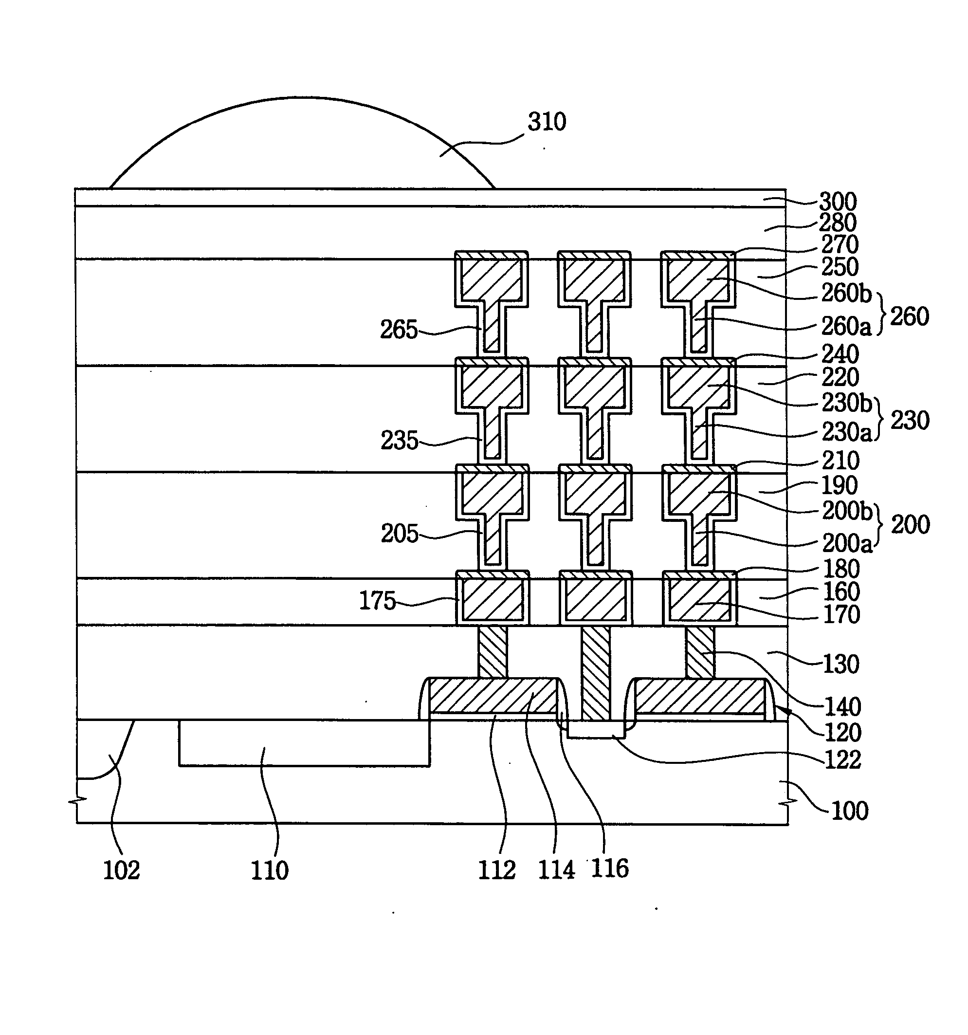
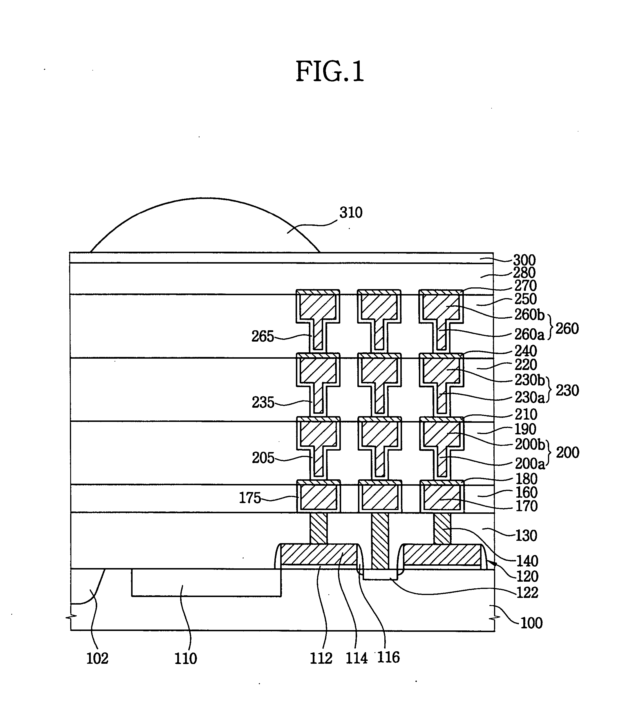
[0039]FIG. 1 illustrates a cross-section of an image sensor device according to the present invention.

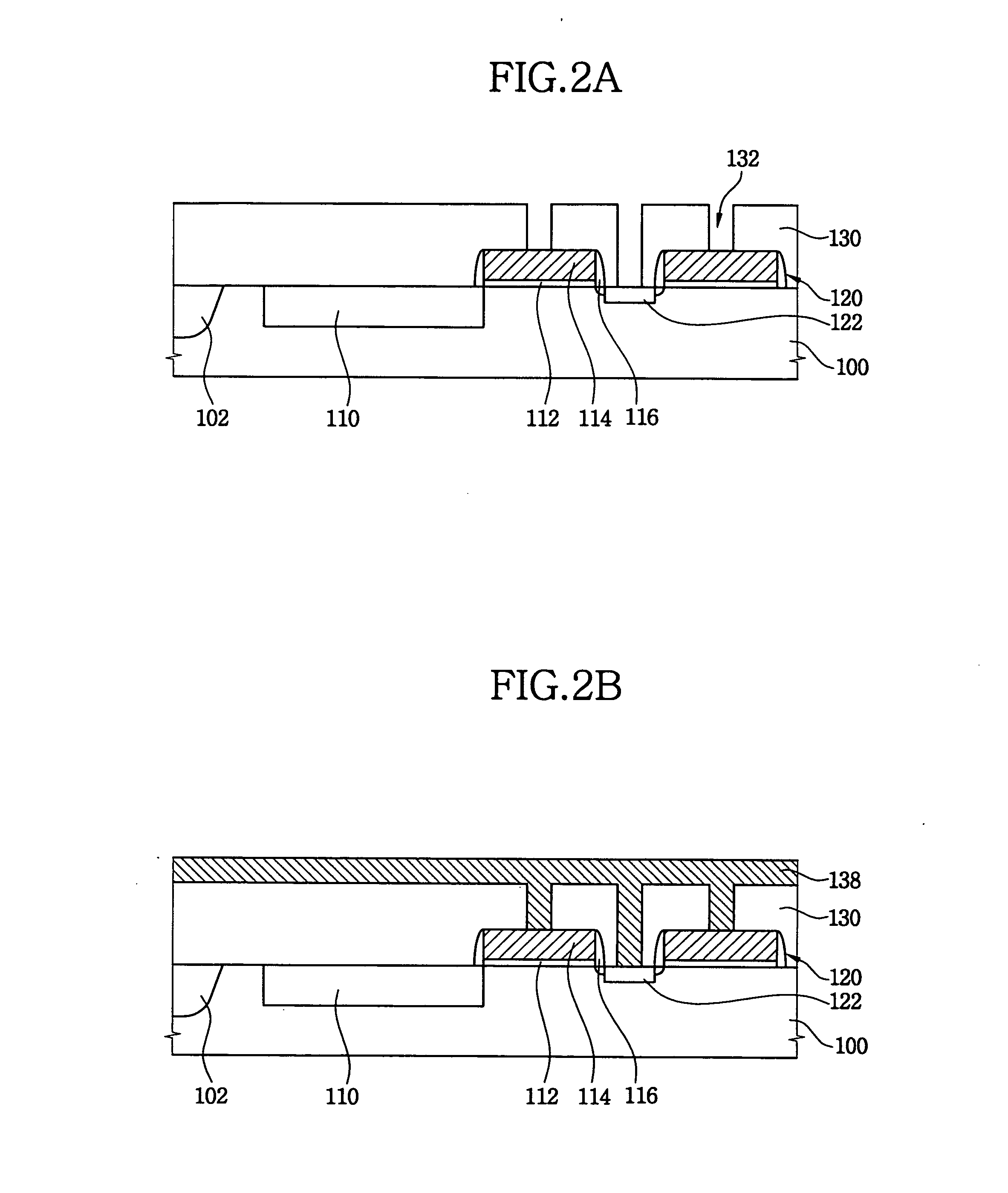
[0040] Referring to FIG. 1, a semiconductor substrate 100 includes an active region defined by a field oxide layer 102. A light-receiving device or photodetector 110, such as a photodiode, is formed on a surface of the active region of the semiconductor substrate 100. Further, transistors 120 serving as a switching device are formed on the semiconductor substrate 100. Each of the transistors 120 includes a gate electrode 114 and source / drain regions 122 formed between one gate electrode 114 and an adjacent gate electrode 114. A gate insulation layer 112 is formed beneath the gate electrode 114, and a spacer 116 is formed on a sidewall of the gate electrode 114.

[0041] A lower insulation layer 130 is formed on the semiconductor substrate 100 on which the transistors 120 are formed. The lower insulation layer 130 includes a transparent material such as silicon oxide. A lower contact 1...

second embodiment

[0097]FIG. 4 illustrates a cross-section of an image sensor device according to the present invention.

[0098] In the image sensor device according to the second embodiment, the upper surfaces of the copper interconnection and the barrier metal pattern are removed to a predetermined depth. Then, the diffusion preventing pattern is formed on the copper interconnection and the barrier metal pattern to fill the removed upper portions of the copper interconnection and the barrier metal pattern. The image sensor device according to this second embodiment has a substantially identical structure as described above regarding the first embodiment, except for a position of the diffusion preventing pattern and a method of forming the diffusion preventing pattern. That is, the above-described diffusion preventing pattern of the first embodiment may be formed by a selective deposition process. However, the diffusion preventing pattern of the second embodiment may be formed by a blanket deposition ...

fourth embodiment

[0137]FIG. 7 illustrates a cross-section of an image sensor device according to the present invention. The image sensor device according to this embodiment has a structure substantially identical to that of the above-described image sensor device except for a patterned anti-reflection coating formed on the photodetector. Thus, detailed descriptions of identical elements will be omitted.

[0138] Referring to FIG. 7, in the image sensor device according to this embodiment, an anti-reflection layer (not shown) is formed over the semiconductor substrate 100 on which the photodetector 110 and the switching device 120 are formed. The anti-reflection layer is patterned to cover the photodetector 110, thereby forming a patterned anti-reflection coating 501. The anti-reflection coating 501 may increase the amount of light incident on the photodetector 110, thus improving performance of the image sensor device. The anti-reflection coating 500 may include SiON, SiC, SiCN, or SiCO. While the part...


PUM


Abstract

In an image sensor device, an insulating interlayer structure having an opening is formed on a semiconductor substrate on which a semiconductor device and a photodetector are formed. An electrically conductive pattern, e.g, copper, fills the opening. A diffusion preventing pattern is formed only on the electrically conductive pattern. A color filter and a lens are also provided in an optical path of the photodetector. The diffusion preventing pattern is not disposed in the optical path of the photodetector. Thus, the image sensor device having the copper pattern may be easily manufactured.

Description

BACKGROUND OF THE INVENTION [0001] 1. Field of the Invention [0002] The present invention relates to an image sensor device. More particularly, the present invention relates to an image sensor device including a complementary metal-oxide-semiconductor (CMOS) image sensor (CIS). [0003] 2. Description of the Related Art [0004] An image sensor converts optical information into electrical signals. Image sensors are generally classified as camera tubes or solid-state devices. The camera tube has been widely used in a variety of technologies, particularly for television, such as measurement, control, and recognition. There are basically two different types of solid-state image sensors: a metal-oxide-semiconductor (MOS) type and a charge-coupled device (CCD) type. [0005] A complementary MOS image sensor (CIS) converts an optical image into an electrical signal using manufacturing technologies for the CMOS. The CIS was developed in the 1960s; however, its development has not progressed much...

Claims


Application Information

Patent Timeline
IPC IPC(8): H01L27/14H01L27/146
CPCH01L27/14621H01L27/14625H01L27/14685H01L27/14683H01L27/14636H01L27/146
Inventor CHOI, SEUNG-MAN
Owner SAMSUNG ELECTRONICS CO LTD
Why Eureka
Try Eureka