High current density electropolishing in the preparation of highly smooth substrate tapes for coated conductors
a technology of electropolishing and high current density, applied in the direction of electrolysis components, superconductor devices, manufacturing tools, etc., can solve the problems of reduced current carrying capacity of superconductive films, processing speeds, and smooth surfa
- Summary
- Abstract
- Description
- Claims
- Application Information
AI Technical Summary
Benefits of technology
Problems solved by technology
Method used
Image
Examples
example 1
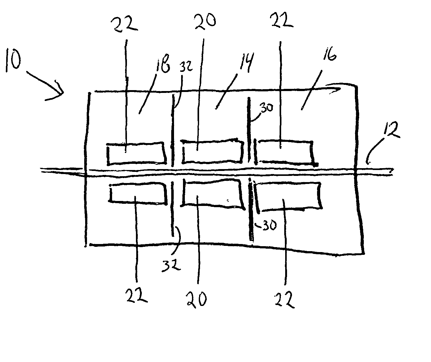
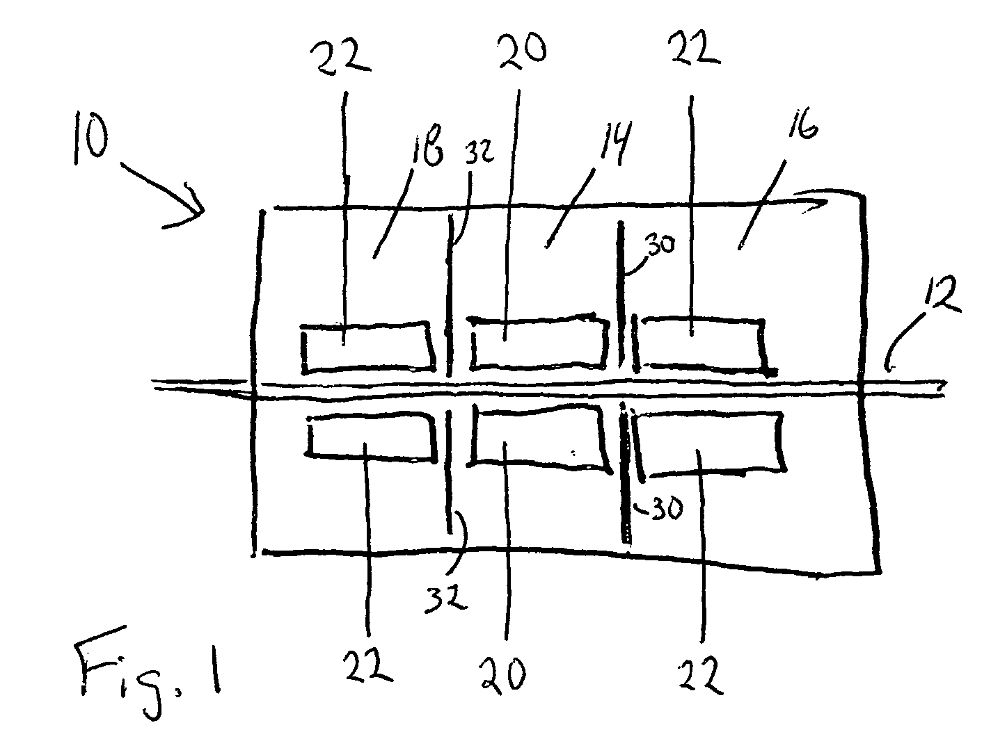
[0036] For the electropolishing of Hastelloy C276 nickel based tape, the tape can be run through the circulating acid bath at speeds between about 10 and 67 centimeters per minute (cm / min), generally about 20 cm / min. The acid bath can include a mixture of highly concentrated sulphuric acid and phosphoric acid. After the polishing step, the tape was rinsed several times with deionized water at room temperature. Finally, the tape was dried in an air stream. The acid temperature was maintained at 70° C. With the equipment system as originally obtained from the manufacturer (Metfab Technologies Inc., Warwick, R.I.), the polishing current was limited to 10 Amperes (A). The tape's surface in the acid was approximately 60 square centimeters (sq-cm); therefore, the resulting mean surface current density on the surface of the tape was limited to a maximum of about 0.17 A / sq-cm. While polishing experiments at this current density and below did show some improvement in smoothness (RMS of above...
example 2
[0038] On a polished substrate (Hastelloy C276) from example 1, was deposited by magnetron sputter deposition a layer of aluminum oxide about 800 to about 1000 Angstroms in thickness. Onto this resultant article was deposited a layer of Y2O3 (about 5 nm) by e-beam evaporation. Onto this resultant article was deposited a layer of MgO about 10 nm in thickness. An ion-assisted, electron beam evaporation system similar to that of Wang et al., App. Phys. Lett., v. 71, no. 20, pp. 2955-2957 (1997), was used to deposit a MgO film upon the yttrium oxide layer. The substrates were ultrasonically cleaned in soap and water, rinsed with deionized water, rinsed with methanol and blown dry with filtered nitrogen. The ion source was manufactured by Ion Tech, Inc. (Ft. Collins, Colo.) with a source geometry of 22 cm by 2.5 cm. The substrate normal to ion-assist beam angle was 45±3°. The ion source gas was argon. The ion source gas was introduced to a background partial pressure of about 1.0×10⁻⁶ To...
example 3
[0039] On the template structure of example 2 was deposited a layer of strontium ruthenate (SrRuO3) about 30 nm in thickness by pulsed laser deposition. Onto the layer of SrRuO3 was deposited a layer of YBCO about 1650 nm in thickness by pulsed laser deposition. The Jc was measured as 1.5×10⁶ A / cm2 using a standard four-point measurement. In the first experiment, the critical current densities in a subsequently deposited YBCO layer on the electropolished tape were comparable to the best results from mechanically polished tape. Better results may be expected through process optimization.
PUM
| Property | Measurement | Unit |
|---|---|---|
| surface current density | aaaaa | aaaaa |
| RMS roughness | aaaaa | aaaaa |
| RMS roughness | aaaaa | aaaaa |
Abstract
Description
Claims
Application Information

