

Ball grid array package substrate and method for manufacturing the same
a technology of grid array and substrate, which is applied in the direction of sustainable manufacturing/processing, final product manufacturing, printed circuit aspects, etc., can solve the problems of weakened shear strength between solder balls and ball pads of the substrate, failure of ball pads, and breakage of the interface between solder balls and the substrate, so as to improve the shear strength of solder balls and improve the wettability of solder balls , excellent shear strength
- Summary
- Abstract
- Description
- Claims
- Application Information
AI Technical Summary
Benefits of technology
Problems solved by technology
Method used
Image

Examples
Embodiment Construction
[0012] Referring to the drawings attached, the present invention will be described by means of the embodiments below.
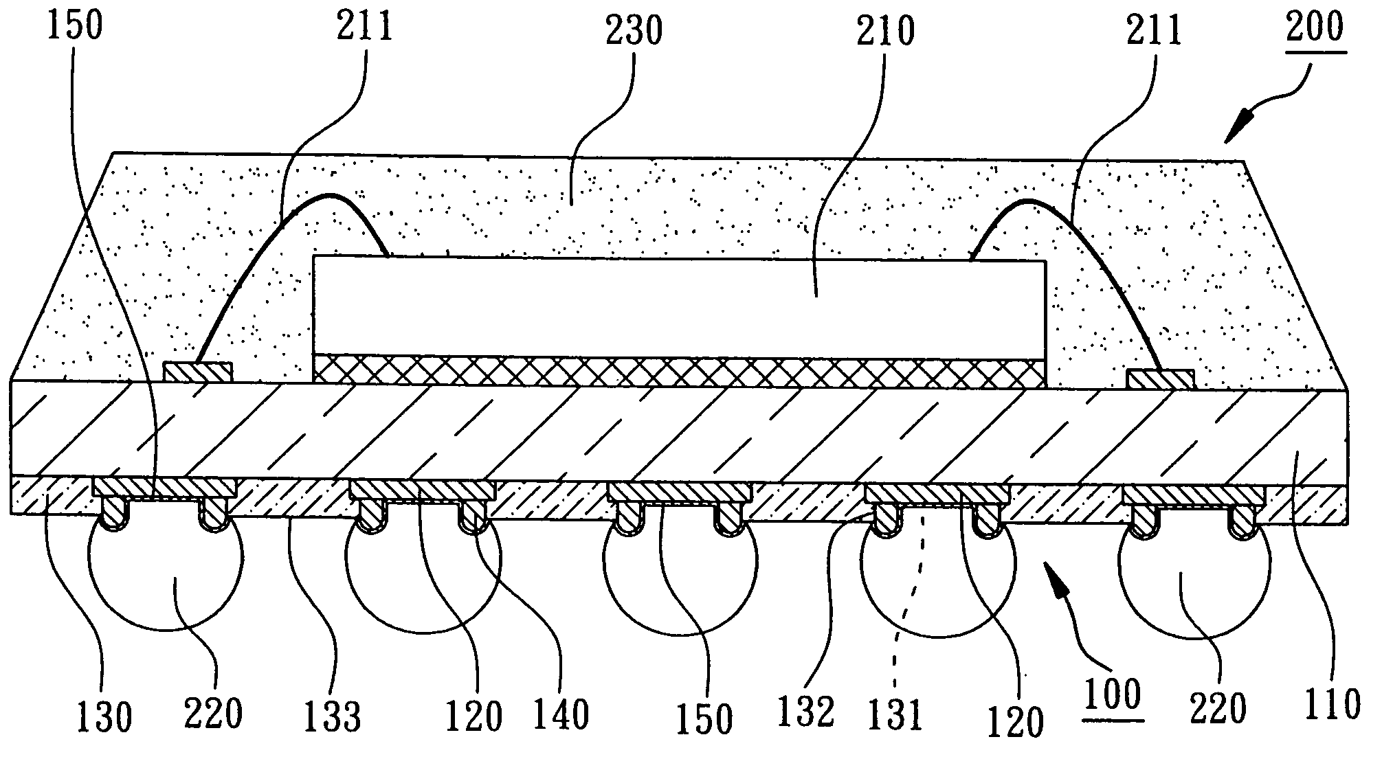
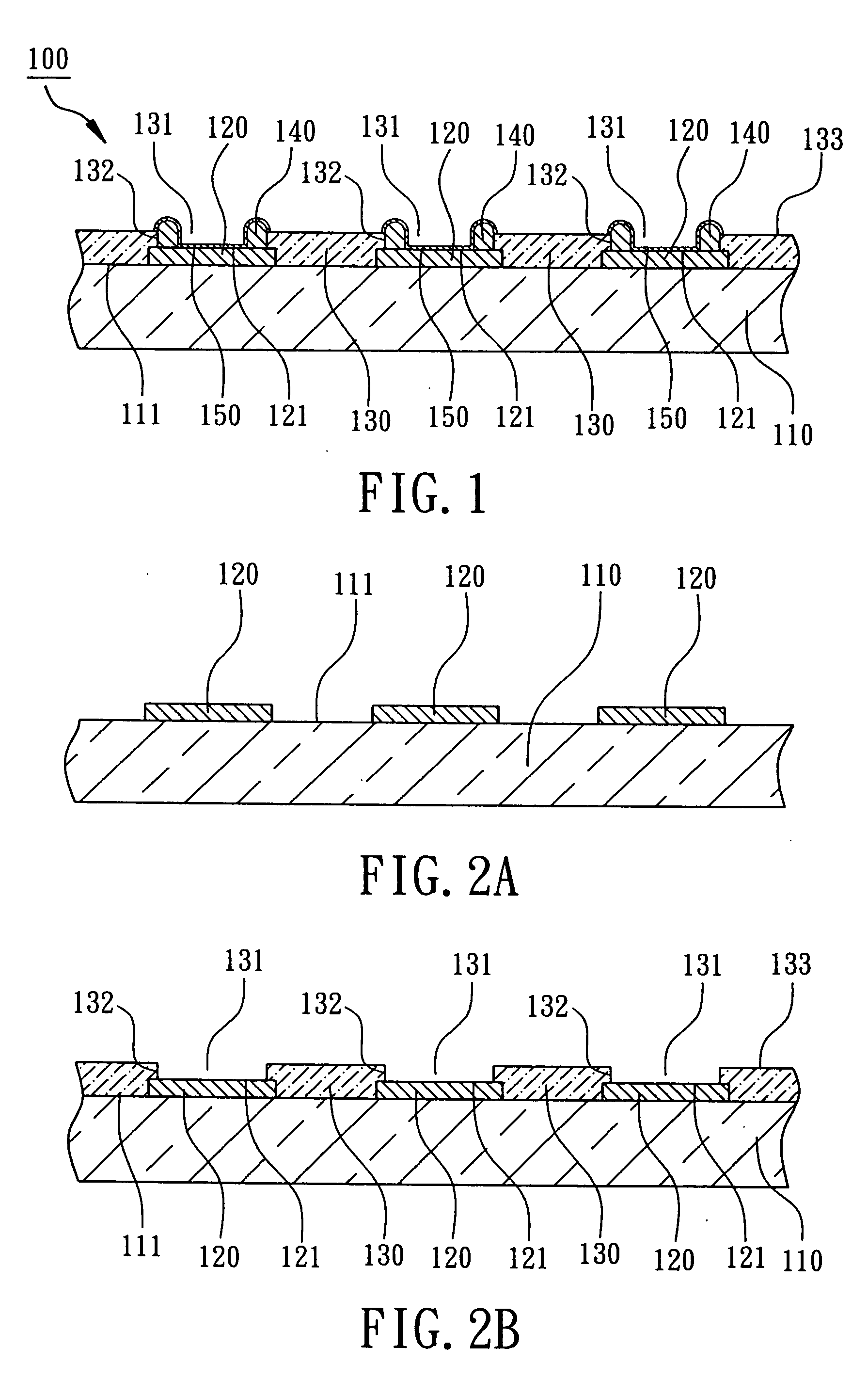
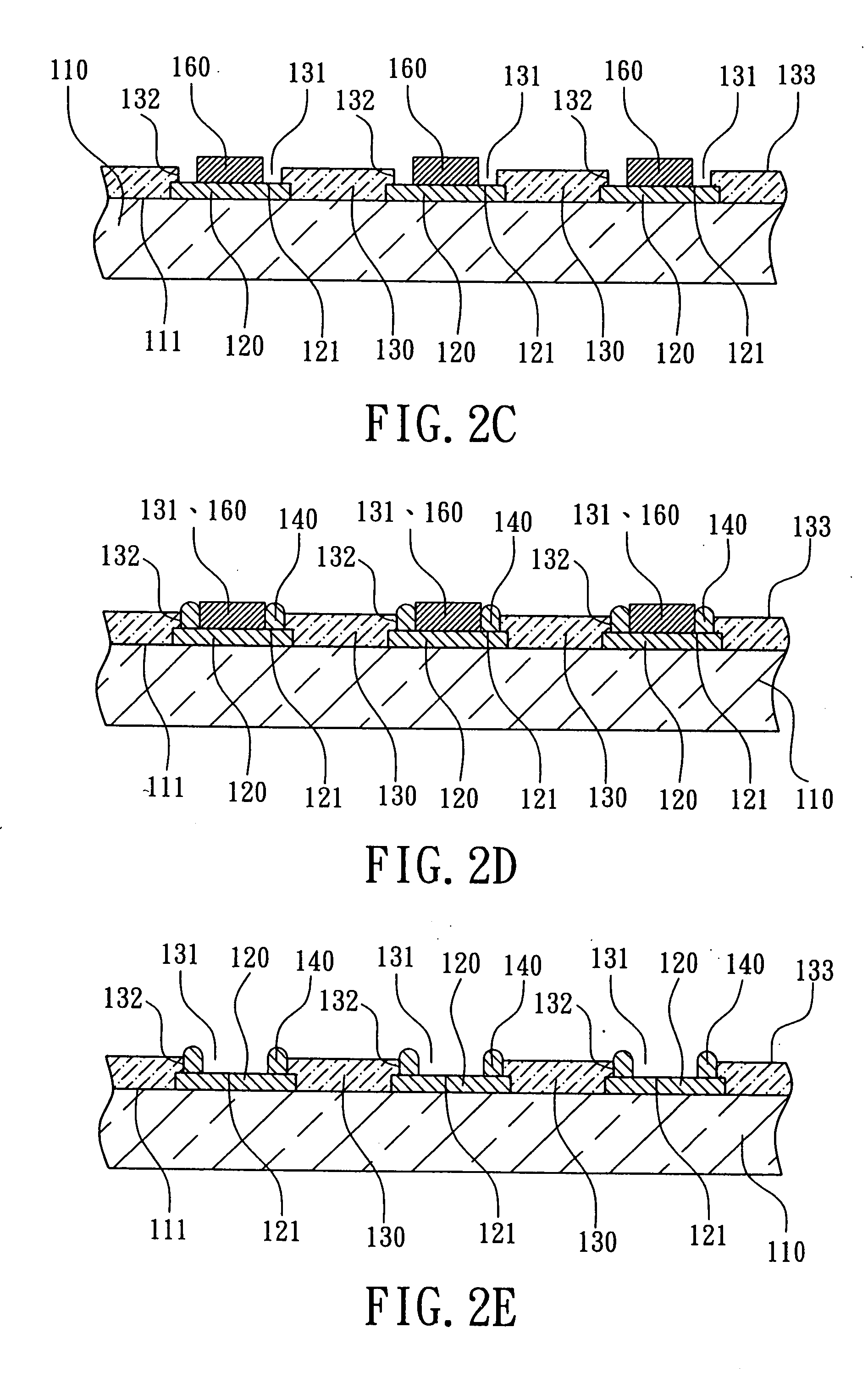
[0013] In accordance with the embodiment of the present invention, a ball grid array package substrate 100 is showed in FIG. 1. The substrate 100 comprises a substrate body 110, a plurality of ball pads 120, a solder mask 130 and a plurality of patterned reinforcing metal layers 140. The substrate body 110 has a surface 111 for SMT connection, the plurality of ball pads 120 and the solder mask 130 are formed on the surface 111 of the substrate body 110. The solder mask 130 has a plurality of openings 131 which partially expose the corresponding ball pads 120 so that each ball pad 120 has an exposed surface 121. Also each opening 131 can be circle or square in shape and has at least a sidewall 132. The patterned reinforcing metal layers 140 are formed on the corresponding ball pads 120 along the sidewalls 132 of the openings 131 of the solder mask 130. Preferably, the...
PUM
 Abstract
Description
Claims
Application Information