Semiconductor device including a semiconductor substrate formed with a shallow impurity region, and a fabrication method for the same

a semiconductor substrate and impurity technology, applied in the direction of semiconductor devices, electrical devices, transistors, etc., can solve the problems of difficult to form a shallow impurity diffused region with a low resistance, difficult to effectively and instantaneously heat up the semiconductor substrate, and difficult to form a shallow pn junction concurrent with the miniaturization of the devi

Inactive Publication Date: 2005-02-03
KK TOSHIBA
View PDF5 Cites 36 Cited by
  • Summary
  • Abstract
  • Description
  • Claims
  • Application Information

AI Technical Summary

Benefits of technology

[0008] An aspect of the present invention inheres in a method for manufacturing a semiconductor device including forming a plurality of isolation regions in a silicon substrate, forming a gate insulator film on the silicon substrate, depositing gate electrodes on the gate insulator film, implanting selectively in the silicon substrate with first impurity ions, annealing to recover crystallographic quality of the implanted silicon substrate suppressing diffusion of the first impurity ions, depositing an interlayer insulator film on the isolation regions, the silicon substrate, and the gate electrodes, and heating the silicon substrate by irradiating a light having a wavelength such that the light is absorbed by the silicon substrate without being absorbed by the interlayer insulator film, to the silicon substrate via the interlayer insulator film, activating the first impurity ions so as to form source and drain regions.

Problems solved by technology

However, formation of a shallower pn junction concurrent with the miniaturization of devices is difficult.
As such, it is difficult to form a shallow impurity diffused region with a low resistance in the semiconductor substrate in which a concentrated impurity can be activated.
Since the light absorbing film formed on the surface of the interlayer insulator film generates heat, while the semiconductor substrate itself does not generate heat, it is difficult to effectively and instantaneously heat up the semiconductor substrate.

Method used


Image

  • Semiconductor device including a semiconductor substrate formed with a shallow impurity region, and a fabrication method for the same
  • Semiconductor device including a semiconductor substrate formed with a shallow impurity region, and a fabrication method for the same
  • Semiconductor device including a semiconductor substrate formed with a shallow impurity region, and a fabrication method for the same

Examples


first embodiment

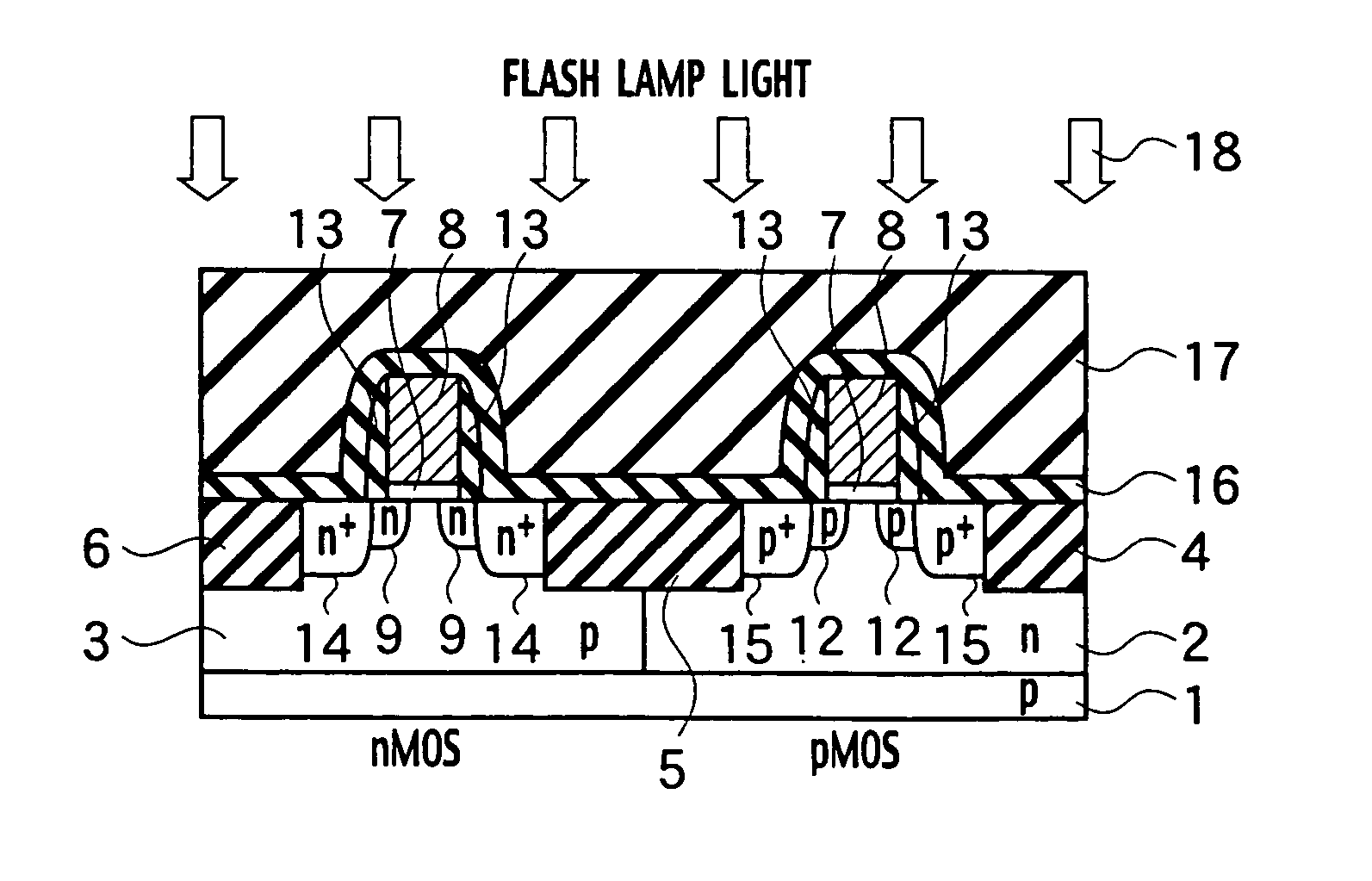
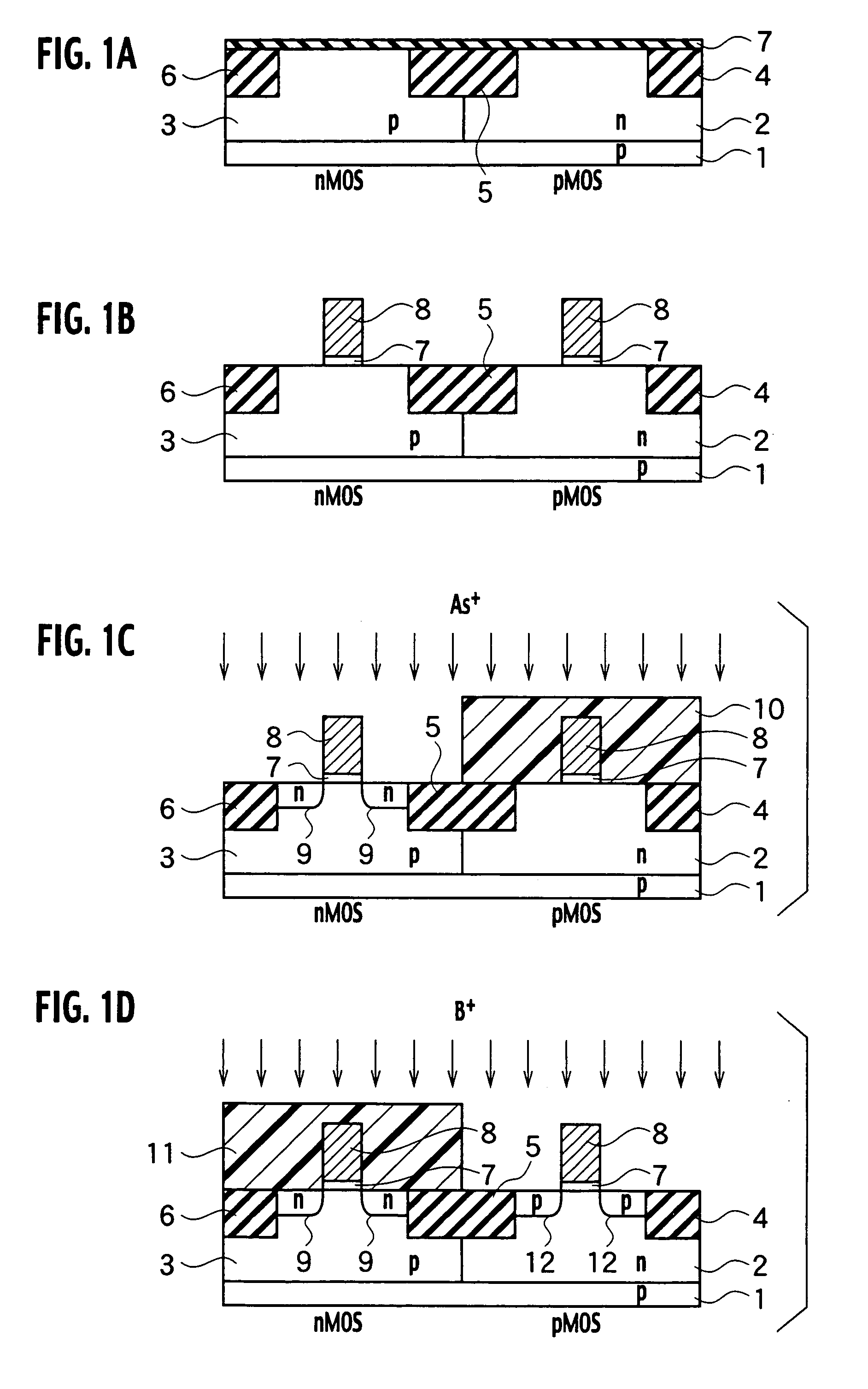
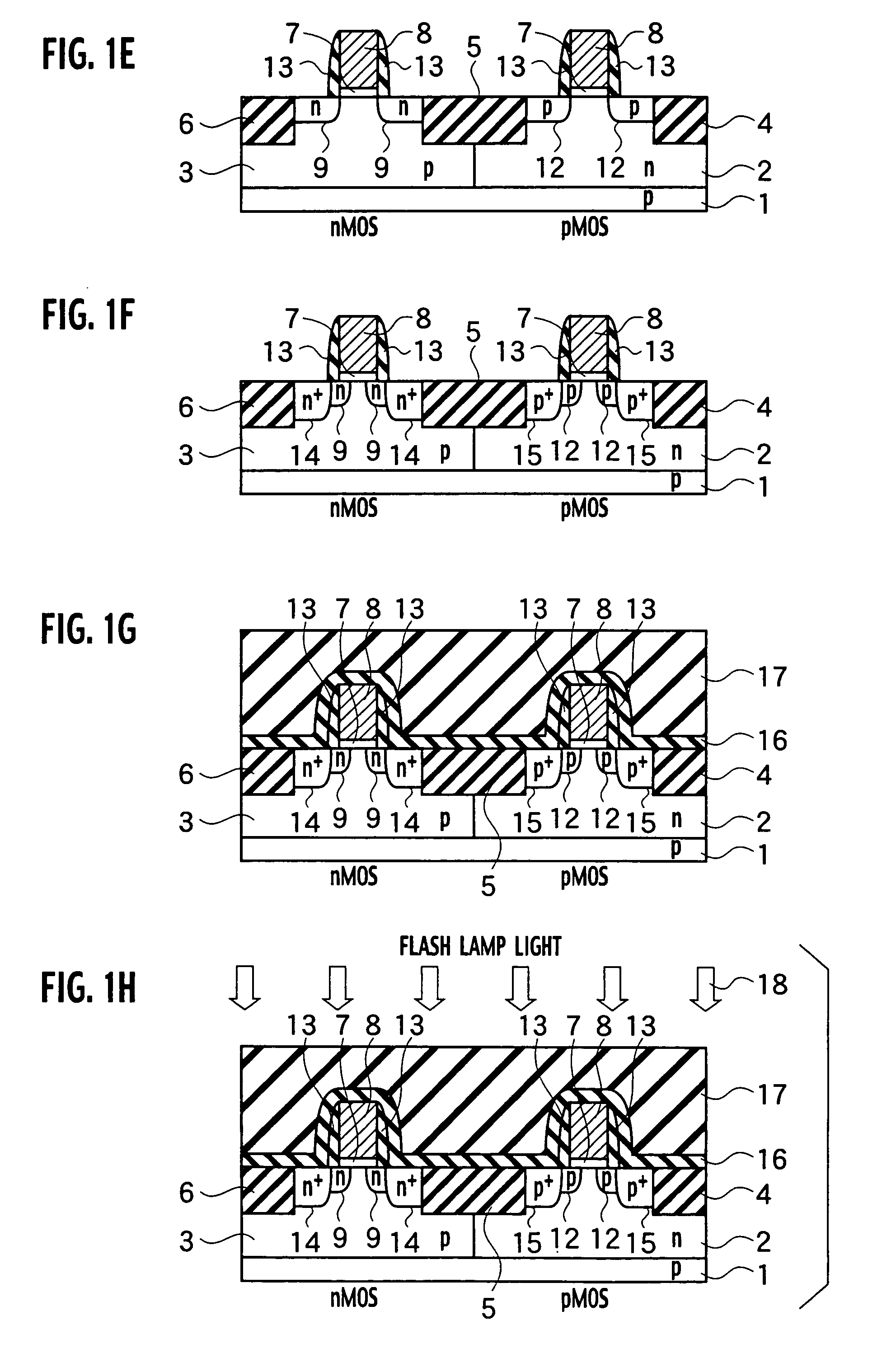
[0033] (First Embodiment)

[0034] A semiconductor device fabrication method according to a first embodiment is described, taking as an example, fabrication steps for CMOS transistors, which form an LSI semiconductor device.

[0035] To begin with, as shown in FIG. 1A, a p-well layer 3 is formed in the nMOS region of a p-type silicon (Si) substrate 1, and an n-well layer 2 is formed in the pMOS region. Isolation regions 4 and 6 are formed around the p-well layer 3 and the n-well layer 2, respectively. Furthermore, a silicon oxide film, to be a gate insulator film 7, is formed on the surface of the p-type silicon substrate 1.

[0036] Next, as shown in FIG. 1B, a polycrystalline silicon film, which becomes gate electrodes 8, is formed on the gate insulator film 7. The polycrystalline silicon film is selectively etched through reactive ion etching (RIE), so as to form the gate electrodes 8.

[0037] As shown in FIG. 1C, a photoresist film 10 is formed on the pMOS region. Using the photoresist ...

second embodiment

[0066] (Second Embodiment)

[0067] A semiconductor device according to a second embodiment is described taking CMOS transistors, which form an LSI semiconductor device, as an example.

[0068] The semiconductor device according to the second embodiment, as shown in FIG. 8, includes a silicon substrate 1, isolation regions 4 through 6 and 37 through 39, gate insulator films 7, gate electrodes 8, source / drain impurity regions 14 and 15, extension impurity regions 9 and 12, and auxiliary layers 35 and 36 that are silicon carbide layers or silicon nitride layers.

[0069] The silicon substrate 1 includes multiple device regions in the nMOS region and the pMOS region. The p-well 3 is deployed on the silicon substrate 1 in the nMOS region. The n-well 2 is deployed on the silicon substrate 1 in the pMOS region.

[0070] The isolation regions 4 through 6 and 37 through 39 are provided on the surface of the silicon substrate 1, isolating the device regions of the nMOS region and the PMOS region. The...

third embodiment

[0098] (Third Embodiment)

[0099] A semiconductor device according to a third embodiment is described taking CMOS transistors, which form an LSI semiconductor device, as an example.

[0100] As shown in FIG. 12, the semiconductor device according to the third embodiment has the silicon carbide layer or silicon nitride layer 35 deployed in a different position from that in the semiconductor device of the second embodiment in FIG. 8. The silicon carbide layer or silicon nitride layer 35 is provided on the underside of the silicon substrate 1.

[0101] A fabrication method for a semiconductor device according to the third embodiment is described taking as an example, fabrication steps of CMOS transistors, which form an LSI semiconductor device.

[0102] To begin with, as shown in FIG. 13A, the silicon carbide layer or silicon nitride layer 35 is formed on the underside of the silicon substrate 1 through plasma CVD. The thickness of the silicon carbide layer or silicon nitride layer 35 is set t...


PUM


Abstract

A method of manufacturing a semiconductor device includes forming isolation regions, a gate insulator film and gate electrodes, implanting in the silicon substrate with impurity ions, annealing to recover crystallinity of the implanted silicon substrate without diffusing the impurity ions, depositing an interlayer insulator film on the isolation regions, the silicon substrate, and the gate electrodes, and heating the silicon substrate by irradiating a light having a wavelength that the light is absorbed by the silicon substrate without being absorbed by the interlayer insulator film, activating the impurity ions so as to form source and drain regions.

Description

CROSS REFERENCE TO RELATED APPLICATIONS [0001] This application is based upon and claims the benefit of priority from prior Japanese Patent Applications No. P2003-172239, filed on Jun. 17, 2003; the entire contents of which are incorporated herein by reference. BACKGROUND OF THE INVENTION [0002] 1. Field of the Invention [0003] The present invention relates to a fabrication method for a semiconductor device for conducting heat treatment on a semiconductor device using a high-intensity light source, and the semiconductor device subjected thereto. [0004] 2. Description of the Related Art [0005] Improvement in performance of a large-scale integration (LSI) semiconductor device, is achieved by increasing the scale of integration. In other words, LSI performance may be improved through miniaturization of devices configuring the semiconductor device. As a result, the LSI is increased to a larger scale, and the devices are miniaturized. In addition, for device miniaturization, a shallow pn...

Claims


Application Information

Patent Timeline
Patent Type & Authority Applications(United States)
IPC IPC(8): H01L21/02H01L21/265H01L21/336H01L21/8238H01L27/092H01L27/12H01L29/78H01L29/786
CPCH01L21/823814
Inventor ITO, TAKAYUKI
Owner KK TOSHIBA
Why Eureka
Try Eureka