LSI device etching method and apparatus thereof

a technology of etching method and etching method, which is applied in the direction of electrical equipment, semiconductor/solid-state device manufacturing, basic electric elements, etc., can solve the problem of monotonous etching speed of sic, which is the film to be etched, and achieve the effect of reducing monotonous etching speed

Inactive Publication Date: 2005-02-03
HITACHI HIGH-TECH CORP
View PDF4 Cites 246 Cited by
  • Summary
  • Abstract
  • Description
  • Claims
  • Application Information

AI Technical Summary

Benefits of technology

[0031] The addition of another adhesive gas (a rare gas such as He, Ne, Ar, or Xe) can change the degree of dissociation and the composition ratio (between radical and ion), so as to control the etching selectivity, etching rate, and pattern, thereby realizing a desired process.

Problems solved by technology

In this case, however, the etching speed of SiC, which is the film to be etched, decreases monotonously.

Method used


Image

  • LSI device etching method and apparatus thereof
  • LSI device etching method and apparatus thereof
  • LSI device etching method and apparatus thereof

Examples


example 1

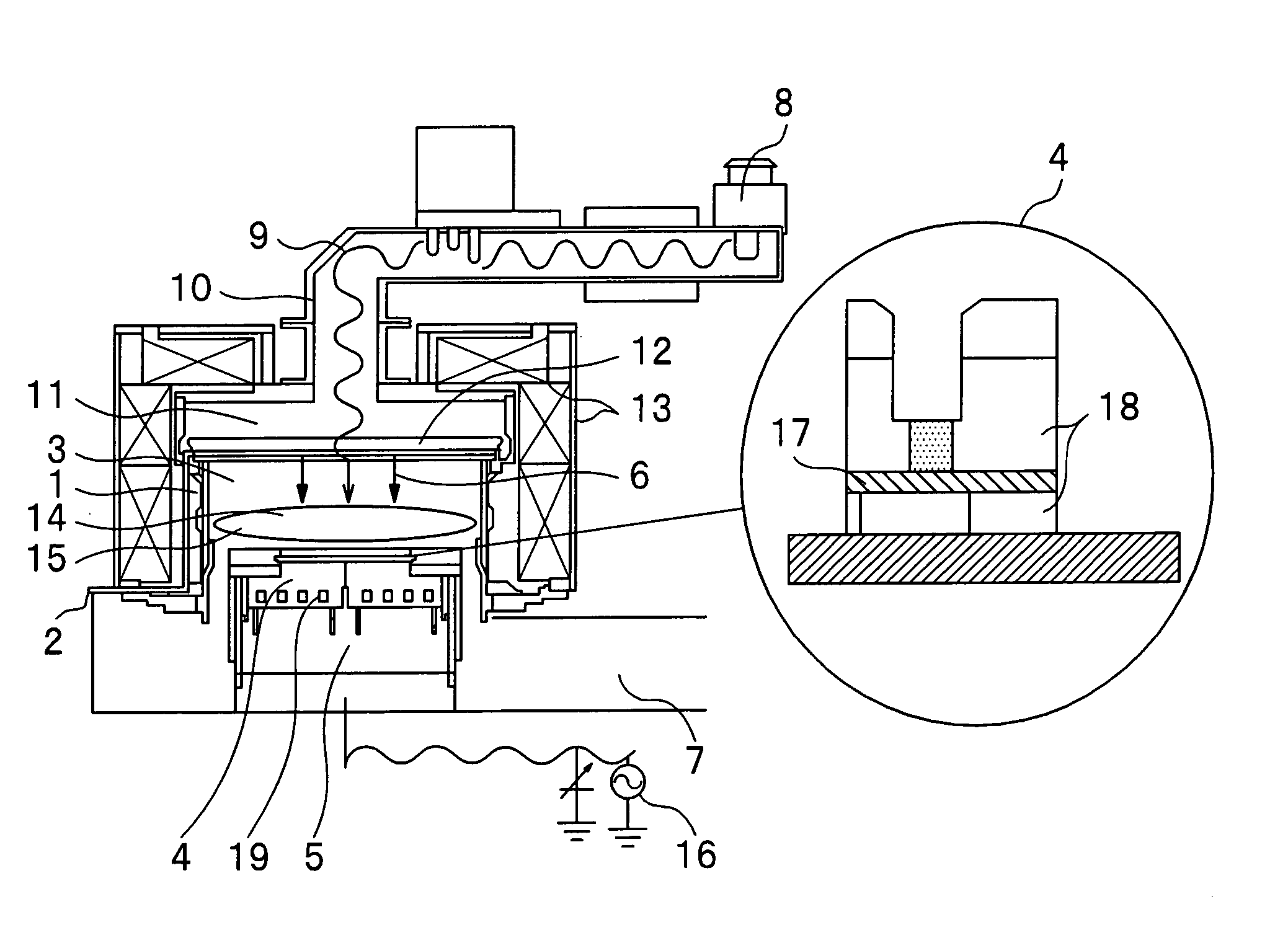
[0110] A first example of the present invention will be described with reference to the plasma treatment apparatus shown in FIG. 1 and the LSI device structure shown in FIG. 3.

[0111]FIG. 3 shows the LSI device structure of an object to be processed, which includes: an underlying interconnection layer (Cu interconnection); a diffusion prevention layer (SiC) formed on the underlying interconnection layer; a low-k film (SiOC) served as an interlayer insulator film layer; a via hole; and an interconnection trench.

[0112] This multilayer interconnection structure (damascene structure) will be supplied using a plasma-etching technique.

[0113] In this example, SiOC is used for the low-k film, but SiOR (R: CxFy wherein x and y are integers), SiON or the like can be used instead of SiOC. Additionally, SiC is used for the diffusion prevention layer, but SiR (R: CxFy wherein x and y are integers), SiCN or the like can be used instead of SiC.

[0114] The plasma treatment apparatus etches the ob...

example 2

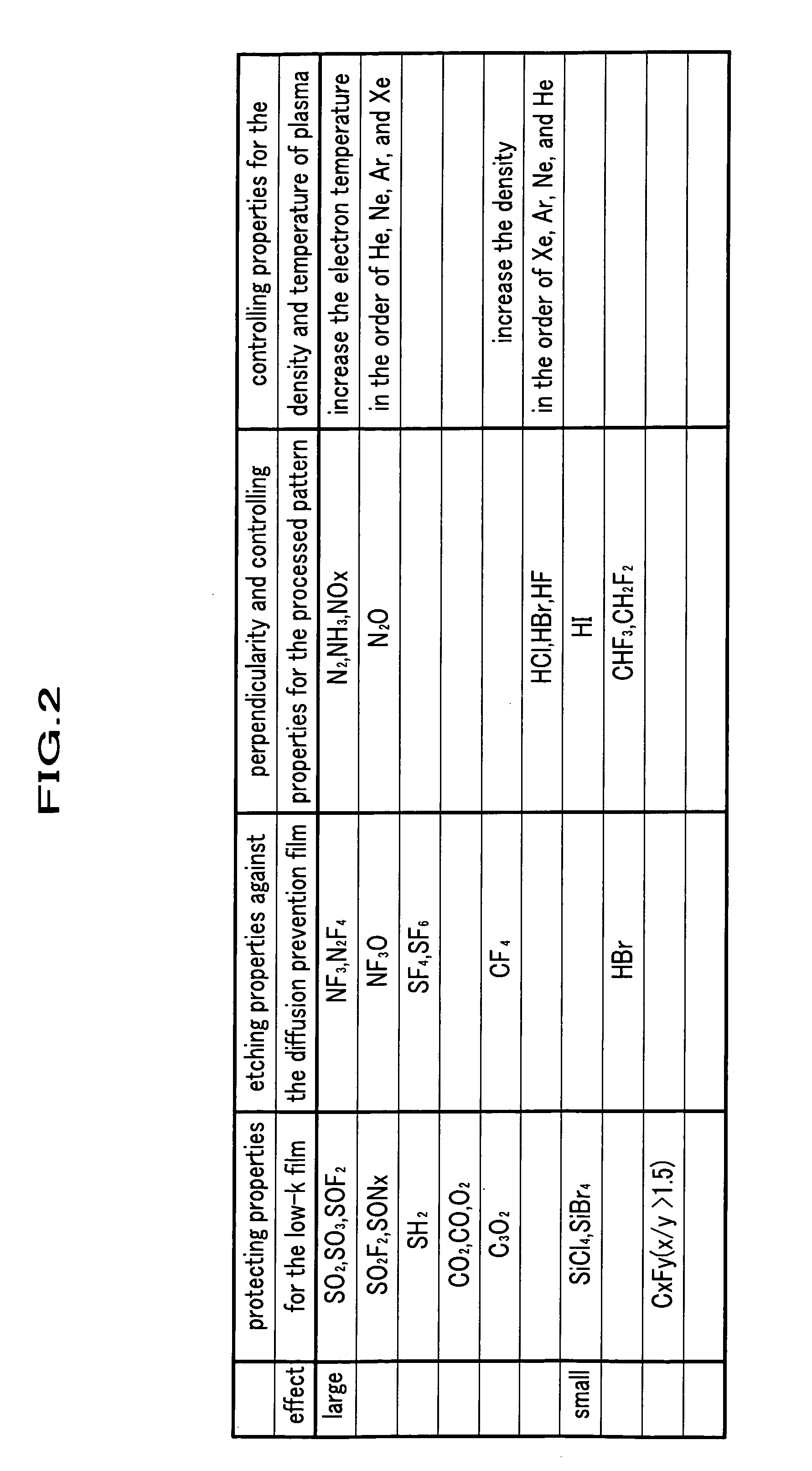
[0125]FIG. 5 shows the LSI device structure of a second embodiment. In this LSI device structure, the mask material 21 is made from SiC, the underlying low-k film 18 is made from SiOC, and the resist 22 is made from C, H, O, or the like. In this embodiment, since SO2 is used as the etching gas, the mask 21 is selectively etched against the low-k film 18 and the resist 22. In this case, gases of SO3, SO, S2O3, SOF2, SO2F2, SONx, SONxFy, or SH2 can be used in addition to SO2.

example 3

[0126] In this example, a gas of NF3 having high etching properties against the diffusion prevention film is mixed with the etching gas of SO2 in order to improve the etching rate. It is also possible to use NF3O, N2F4, or SF6 in place of NF3 to be mixed with the etching gas SO2.

[0127] In the etching apparatus shown in FIG. 1, as the etching gas, SO2 and NF3 are mixed at a ratio of 1:2 and this mixture gas is supplied from the gas introduction system 2. Here, the power of the microwave is set to 800 W, and the pressure and the RF are used as parameters. In this case, the etching rate of SiC was up to 350 nm / min, and the etching selectivity of SiC to SiOC was 5 to 15.

[0128] According to the present example, (1) the improved etching selectivity of the diffusion prevention film against the low-k film and (2) the improved etching rate are obtained, in addition to protecting properties of the low-k film by the etching gas explained in example 1. This combination of the mixed gas can al...


PUM


Abstract

An apparatus for performing a plasma-etching of a LSI device including a Cu interconnection, a low-k film, and a diffusion prevention film has a treatment chamber, into which an etching gas is introduced, and a support table which is equipped with electrodes and on which said LSI device is placed. In this apparatus, the etching gasses are turned into plasma by supplying radio frequency power to electrodes provided within the treatment chamber, so that the LSI device is etched with ions of the plasma. In this apparatus, a sulfur-containing gas and a fluorine-containing gas are mixed to the etching gasses, so that the diffusion prevention film is selectively etched against the low-k film.

Description

BACKGROUND OF THE INVENTION [0001] 1. Field of the Invention [0002] The present invention relates to an LSI device etching method and apparatus for treating LSI devices by making use of plasma. [0003] 2. Description of Relevant Art [0004] With the rapid advancement in finer sizes and higher integration, LSI devices with a gate length of 0.13 μm have been shifted to mass production, and LSI devices with sizes of 90 or 65 nm are being developed. For high speed operation of LSI devices, it is necessary to achieve an improvement in the operation speed of the transistors and to overcome the propagation delay (so-called RC delay) of multilayer metal interconnection. In recent years, the propagation delay of interconnection is becoming more and more influential. [0005] As a solution means, Cu interconnection having a low resistivity ρ and a low-k film having a low relative permittivity k of the capacitor part are being developed. Since CuClx, a chloride of Cu, is low in steam pressure, pla...

Claims


Application Information

Patent Timeline
Patent Type & Authority Applications(United States)
IPC IPC(8): H01L21/311H01L21/3065H01L21/3213H01L21/44
CPCH01L21/31116
Inventor KAZUMI, HIDEYUKIYOSHIDA, TSUYOSHIIKEGAMI, EIJINAKAUNE, KOUICHISAKAGUCHI, MASAMICHIMIYAMOTO, YASUYUKISANO, AKIHIRO
Owner HITACHI HIGH-TECH CORP
Why Eureka
Try Eureka