Semiconductor production method

a production method and semiconductor technology, applied in the direction of semiconductor devices, semiconductor/solid-state device details, electrical apparatus, etc., can solve the problems of deteriorating insulation reliability between interconnects, and achieve the effect of preventing deterioration of copper interconnects and device reliability

Inactive Publication Date: 2005-02-10
HITACHI LTD
View PDF7 Cites 50 Cited by
  • Summary
  • Abstract
  • Description
  • Claims
  • Application Information

AI Technical Summary

Benefits of technology

The present invention adopts electroless plating to deposit an electroconductive capping (metal) layer on a copper interconnect, wherein the protective film is selectively deposited on the copper interconnect while preventing penetration of a plating solution into the dielectric film in which the copper interconnect is provided, to prevent deterioration of copper interconnect and device reliability.

Problems solved by technology

As discussed above, the conventional electroless plating methods for depositing a capping (metal) layer involve problems related to selective deposition, e.g., the film may not be deposited to totally cover copper, or may be deposited on a dielectric film in addition to the interconnect (see FIG. 7), to deteriorate insulation reliability between the interconnects.

Method used


Image

  • Semiconductor production method
  • Semiconductor production method
  • Semiconductor production method

Examples


example 1

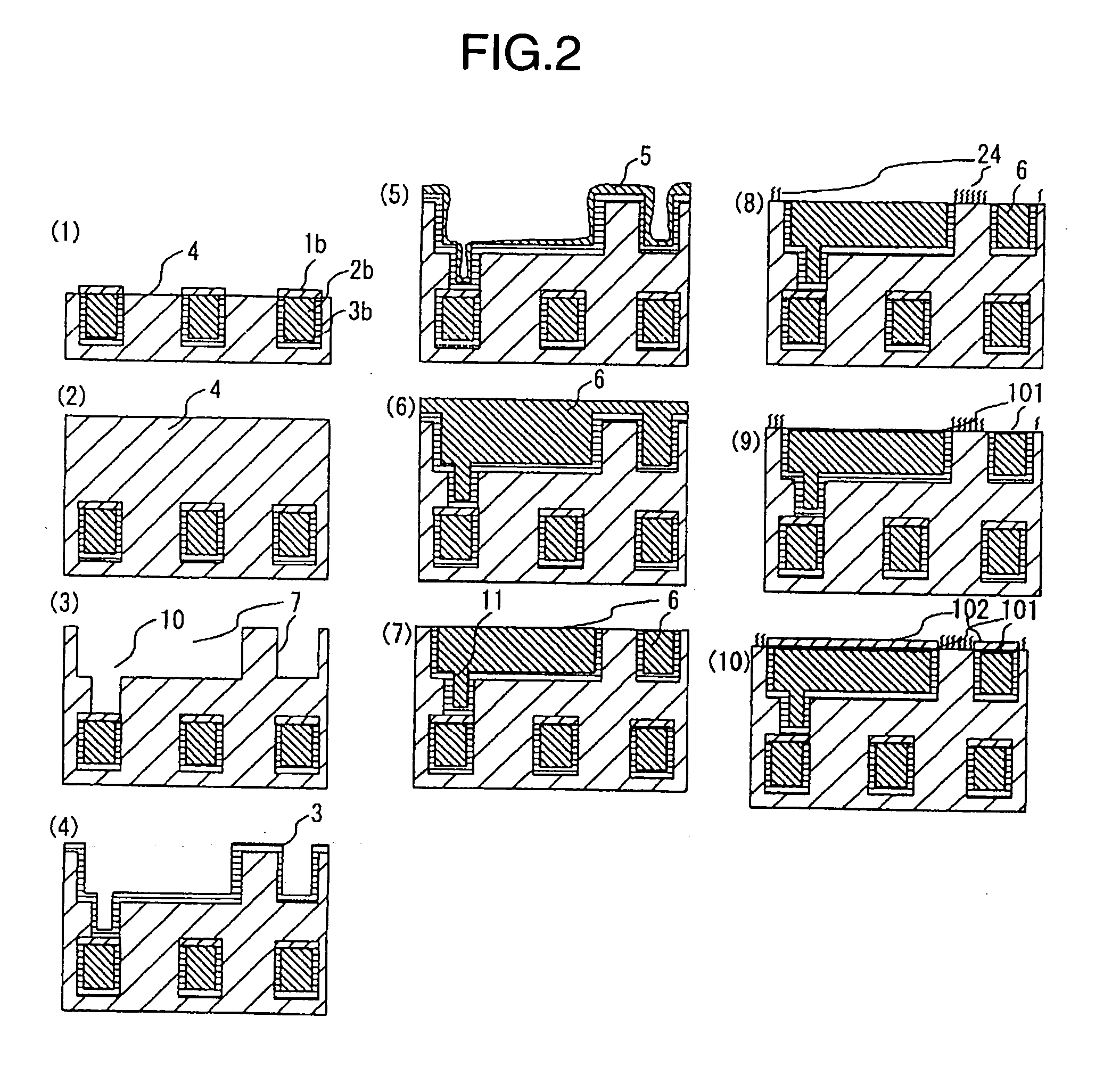
EXAMPLE 1 is described by referring to FIG. 2. A 200 mm-diameter silicon substrate was provided with the devices of the lower copper interconnect 2b (FIG. 2(1)), and then with the SiO2 dielectric film 4 to a thickness of 1 μm by a known CVD procedure (FIG. 2(2)). The dielectric film was porous with a number of 3 nm-diameter holes. Then, the wiring grooves 7 and connection holes 10 were provided by dry etching (FIG. 2(3)), where the wiring groove was 0.3 μm wide and connection hole was 0.3 μm in diameter. Then, TA was formed into a 50 nm thick film by sputtering to serve as the barrier film 3 (FIG. 2(4)), and copper was formed into a 150 nm thick film to serve as the copper seed layer 5 (FIG. 2(5)). The copper seed layer 5 was formed by a long-distance, Cu-sputtering apparatus (Nippon Shinku Gijutsu, Co., Ltd., CERAUSZX-1000) at a film-making speed of 200 to 400 nm / minute. The coated substrate was immersed in the plating solution, described below, and plated under the conditions of ...

examples 2 to 6

, and Comparative Examples 1 to 2

In EXAMPLES 2 to 6, the dielectric substrate described in Table 1 was coated with the layers, where the combination of the plating pretreatment steps was changed to evaluate the selective deposition. The semiconductor was prepared in each of EXAMPLES following the procedure similar to that for EXAMPLE 1. The dielectric film 4 prepared in each of EXAMPLES 4 to 6 and COMPARATIVE EXAMPLE 1 was not porous. Selectivity was evaluated by SEM analysis and elementary analysis based on energy dispersion X-ray (EDX) spectroscopy according to the following patterns. Evaluation of undeposited part 100 holes, 0.12 μm in diameter, in a dot-shape pattern

Abnormal Deposition on the Dielectric Film between the Interconnects 100 lines in a line-and-space pattern, 0.15 μm wide, where the dielectric film surface between the 2 lines was observed

Abnormal Deposition in the Porous Dielectric Film 100 lines in a line-and-space pattern, 0.15 μm wide, where the dielectri...

example 7

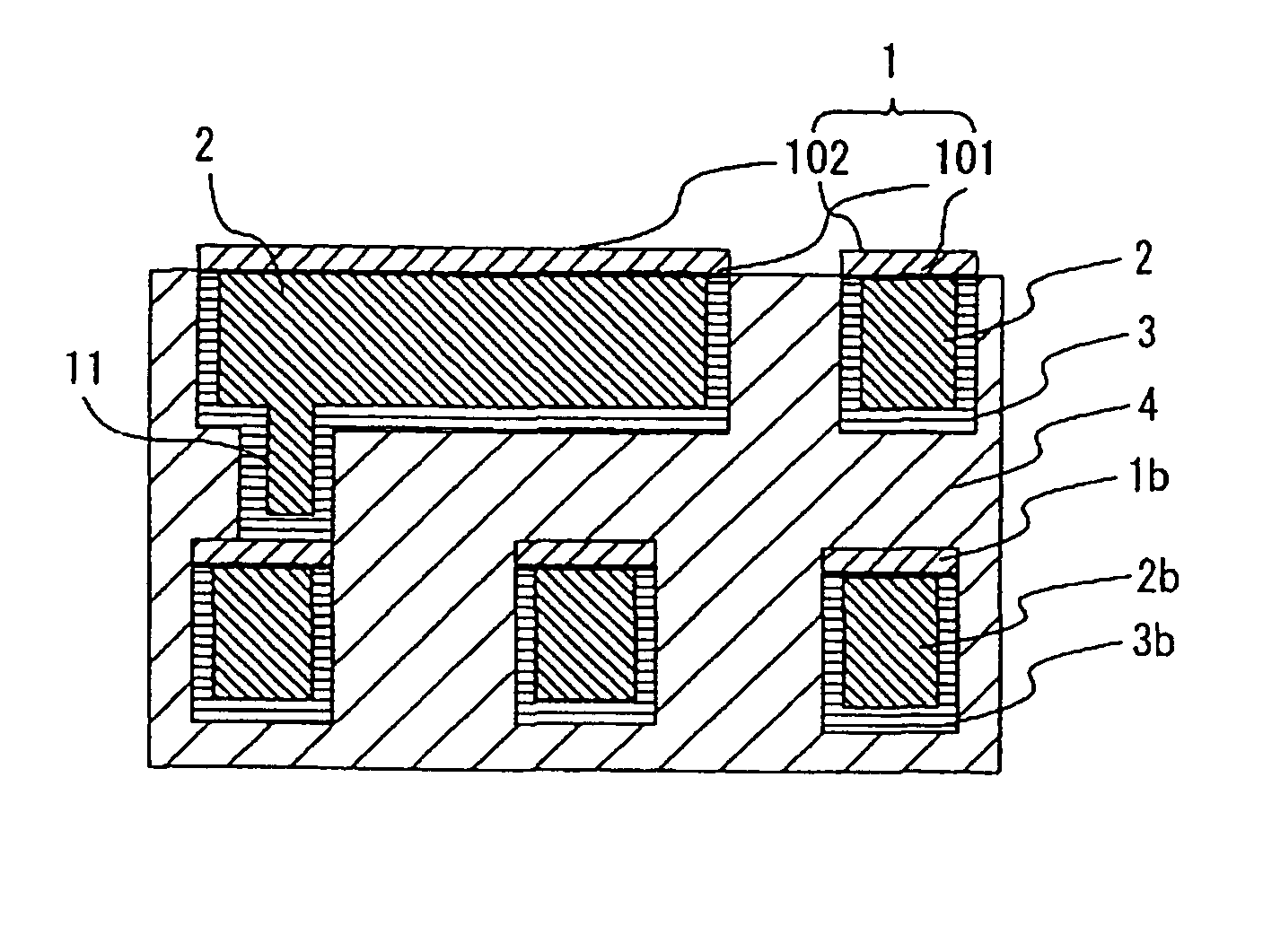
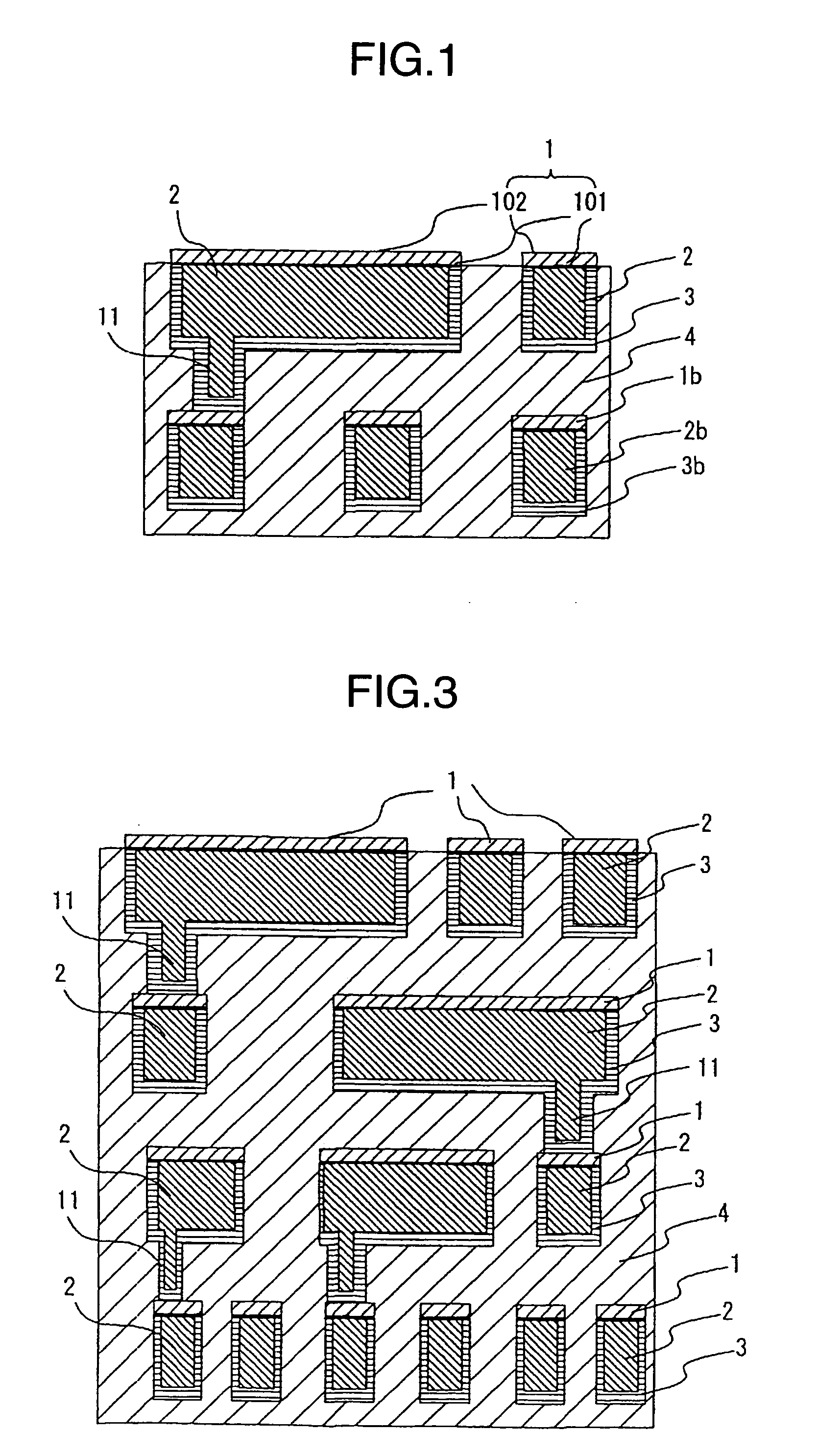
In EXAMPLE 7, the capping (metal) layer 1 was prepared in a manner similar to that for EXAMPLE 1, and evaluated by a life test. The semiconductor prepared in EXAMPLE 7 was provided with a 4-layered capping (metal) layer, as illustrated in FIG. 3, prepared by repeating cycles of the steps (1) to (10) shown in FIG. 2. The life test measured reliability of the dielectric film and interconnect resistance increase after 600 and 1200 hours of service. Interconnect shape (A) Line width: 0.13 μm (B) Film thickness: 0.8 μm (C) Interconnect length: 2.5 mm

Test Conditions (A) Temperature: 175° C. (B) Current density: 3×10⁶ A / cm2

Interconnect resistance increased by 2% after 600 hours and 5% after 1200 hours. No dielectric breakdown was observed after 1200 hours.

It was thus demonstrated that the semiconductor of this embodiment was stable over a long period of time. The reliability test with a voltage applied to the semiconductor also has confirmed the effect of the present invention ...


PUM

PropertyMeasurementUnit
dielectric constantaaaaaaaaaa
thicknessaaaaaaaaaa
diameteraaaaaaaaaa

Abstract

It is an object of the present invention to provide a semiconductor device production method in which an electroconductive capping (metal) layer is formed on a copper interconnect surface, wherein the capping (metal) layer is selectively formed to produce the semiconductor device of high reliability. In the semiconductor device production method, a capping (metal) layer is formed on a copper interconnect in a semiconductor integrated circuit, a first capping (metal) layer is formed by electroless plating with a plating solution containing a reducing agent active on a copper interconnect surface, and then a second capping (metal) layer is formed by another electroless plating.

Description

FIELD OF THE INVENTION The present invention relates to a semiconductor device production method, more particularly a method for forming a capping (metal) layer. BACKGROUND OF THE INVENTION Higher operating speed of devices for a semiconductor have been required to achieve higher degree of integration and higher performance, which has been promoting further miniaturization and layer multiplication of internal wiring of LSIs. The miniaturization and layer multiplication increase interconnect resistance and also inter-wiring capacitance, and affect signal transfer speed in the interconnects. The resulting signal transfer delay time limits operational speed of the device. Therefore, the operational speed has been improved by lowering dielectric constant of the interlayer dielectric film to control capacity between the interconnects, and decreasing resistance of the interconnect material to decrease interconnect resistance. Consequently, attempts have been made to use copper having a...

Claims


Application Information

Patent Timeline
Patent Type & Authority Applications(United States)
IPC IPC(8): H01L21/3205H01L21/288H01L21/768H01L23/52
CPCH01L21/288H01L21/76874H01L21/76849
Inventor NAKANO, HIROSHIITABASHI, TAKEYUKIAKAHOSHI, HARUO
Owner HITACHI LTD
Why Eureka
Try Eureka