High frequency circuit module

a high-frequency circuit and circuit module technology, applied in the direction of waveguides, instruments, semiconductor/solid-state device details, etc., can solve the problems of inability to suppress the occurrence of electromagnetic waves propagating between a plurality of grounding layers, the effect of reducing the area occupied by the rf circuit, improving the resistance to distortion and destruction by a mechanical stress moment of the multi-layer substrate, and facilitating assembly work

Inactive Publication Date: 2005-02-10
HITACHI LTD
View PDF7 Cites 37 Cited by
  • Summary
  • Abstract
  • Description
  • Claims
  • Application Information

AI Technical Summary

Benefits of technology

[0016] According to the invention, a millimeter wave transmission line extending vertically to a layer with a small transmission loss is provided in a hard multilayer dielectric substrate, and a metal layer for a DC / IF signal is shielded by grounding metal layers in the substrate. With the configuration, crosstalk to a DC / IF signal of a millimeter wave signal is lessened, the area occupied by the RF circuits can be reduced by multilayer wiring of the RF circuit, and resistance to distortion and destruction by a mechanical stress moment of the multilayer substrate is improved. Further, the surface of the multilayer dielectric substrate is flat and the assembling work is easily made by one-side reflowing, so that a small, thin, and low-cost RF circuit module can be realized. Particularly, the invention is effective to realize an automotive radar module having excellent cost efficiency and resistance to vibration, which is requested to have high performance.

Problems solved by technology

However, when electromagnetic coupling slots are provided above and below the microstrip line, a potential difference occurs between the upper and lower slot metallic layers.
An amount corresponding to the energy of the electromagnetic wave becomes a loss, so that it difficult to realize the transmission line of a low loss.
However, occurrence of an electromagnetic wave propagating between a plurality of grounding layers cannot be suppressed.
Consequently, the method cannot be used to connect the conductors to realize a low loss in the millimeter wave band.
As described above, the conventional techniques have problems with respect to easiness in manufacture, manufacturing cost, and circuit characteristics.
Although the line length can be shortened by mounting the RF circuit part on the same face of the substrate as the antenna, it is difficult to mount the RF circuit part and the antenna on the same face due to the limited size of the RF circuit part and the hermetic structure.
Consequently, the structure whose assembling and processing cost is high has to be employed.
It makes the millimeter waver radar unstable.
In addition, since the flexibility of designing of layout of the RF circuit is regulated in the two-layer substrate, reduction in cost by reducing the substrate area of the expensive RF circuit part is limited.

Method used


Image

  • High frequency circuit module
  • High frequency circuit module
  • High frequency circuit module

Examples


Embodiment Construction

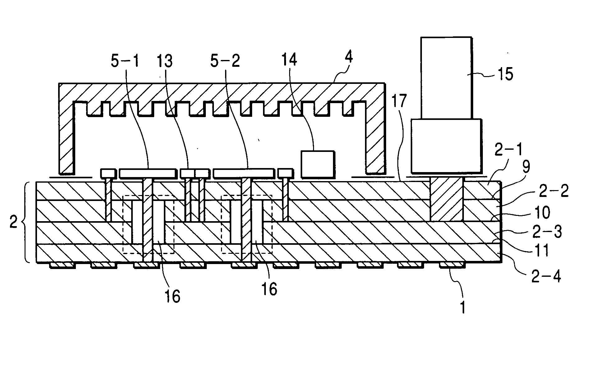
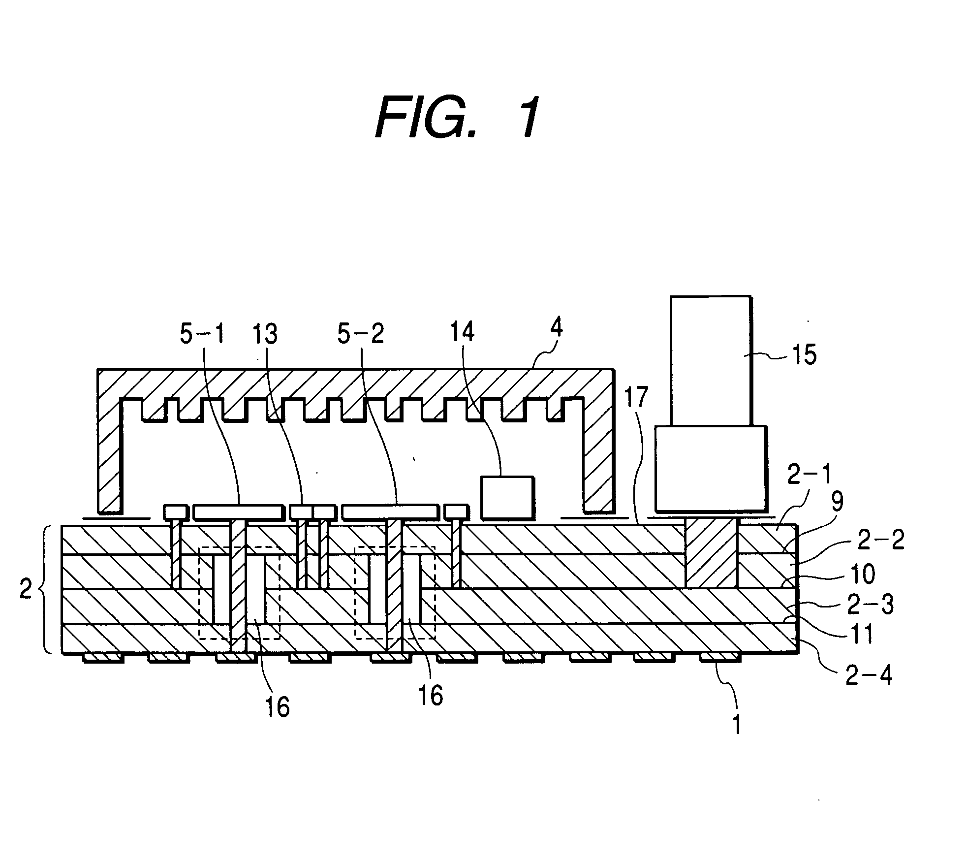
[0029]FIG. 1 is a sectional side view showing the configuration of an example of an RF circuit module according to the invention. In the embodiment, as will be described hereinlater, the RF circuit module is used for an automotive radar using a millimeter wave.

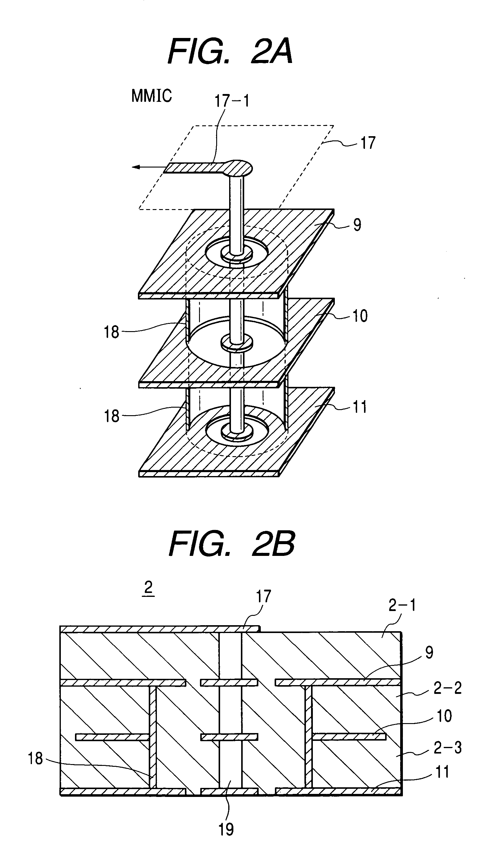
[0030] In a hard multilayer dielectric substrate 2 of the embodiment, four hard dielectric layers 2-1, 2-2, 2-3, and 2-4 are formed, metallic layers 9, 10, and 11 are formed on the layers 2-2, 2-3, and 2-4, respectively, and a metallic pattern 17 is formed on the top face of the layer 2-1. By the metallic pattern 17,. hard dielectric layer 2-1, and metallic layer 9, a transmission line such as a microstrip line is formed. The metallic layer 10 constructs a power providing line and a low frequency signal transmission line, and the metallic line 11 is used as a grounding metallic layer. On the surface of the hard dielectric layer 2-1, RF circuit parts 5-1 and 5-2 such as MMICs are mounted. On the outer face (rear face) of the d...


PUM


Abstract

A high frequency circuit module for use in an automotive radar or the like, in which RF circuit parts are mounted on both sides of a hard multilayer dielectric substrate, and a transmission line connecting the RF circuit parts provided on both sides is constructed by a via group including a periodical structure or a via having a coaxial structure perpendicular to faces of the multilayer dielectric substrate. As the multilayer dielectric substrate, a hard multilayer substrate using metallic layers as a microstrip line wiring layer, a DC/IF signal line layer, and grounding metal layers for shielding which are disposed on and under the DC/IF signal line is employed. By using the transmission line achieved by a through via having the periodical structure or the through via having the coaxial structure, an electromagnetic wave propagating in parallel between the grounding conductors is confined.

Description

BACKGROUND OF THE INVENTION [0001] 1. Field of the Invention [0002] The present invention relates to a high frequency circuit module and, more specifically, to a high frequency circuit module in which a high frequency circuit part such as a monolithic microwave integrated circuit (hereinbelow, called an MMIC) and an antenna are provided on the surface and the rear face, respectively, of a multilayer dielectric substrate. More particularly, the invention relates to a high frequency circuit module suitable for an automotive radar module using millimeter waves. [0003] 2. Description of the Related Arts [0004] As the most effective system of an intelligent transport system (ITS) solving a traffic accident, traffic jam, environmental problems of exhaust gas, noise, and so one, resource problems due to large consumption of oil energy, and the like caused by “vehicles”, a millimeter wave radar has been developed. In order to equip vehicles as many as possible with millimeter wave radars, r...

Claims


Application Information

Patent Timeline
Patent Type & Authority Applications(United States)
IPC IPC(8): H05K3/46G01S7/03G01S13/931H01L23/12H01L23/552H01L23/66H01P1/00H01P1/04H01P3/08H01Q1/32H01Q9/04H01Q21/00H01Q23/00H04B1/38H04B1/3822H05K1/00H05K1/02H05K1/03H05K1/11H05K3/42
CPCG01S7/032G01S2007/028H01L23/552H01L23/66H01L2223/6616H01L2223/6627H01L2223/6677H01L2223/6688H01L2224/48091H01L2224/48227H01L2924/01078H01L2924/01079H01L2924/09701H01L2924/15153H01L2924/1517H01L2924/16152H01L2924/1616H01L2924/16195H01L2924/1903H01L2924/19041H01L2924/19105H01L2924/3011H01L2924/3025H01P1/047H01Q1/3233H01Q9/0407H01Q21/0087H01Q23/00H05K1/0222H05K1/0298H05K1/0306H05K1/115H05K1/116H05K3/429H05K3/4629H05K2201/09618H05K2201/09781H05K2201/09809G01S13/931H01L2924/1423H01L2924/01322H01L24/48H01L2924/00014H01L2924/00H01L2924/12042H01L2224/05599H01L2224/45099H01L2224/85399H01L2924/14H05K1/0221H05K1/0243G01S7/028H01L2224/45015H01L2924/207
Inventor NAGAISHI, HIDEYUKIKONDOH, HIROSHI
Owner HITACHI LTD
Why Eureka
Try Eureka