Semiconductor sensor and method of plating semiconductor devices
- Summary
- Abstract
- Description
- Claims
- Application Information
AI Technical Summary
Benefits of technology
Problems solved by technology
Method used
Image

Examples
Embodiment Construction
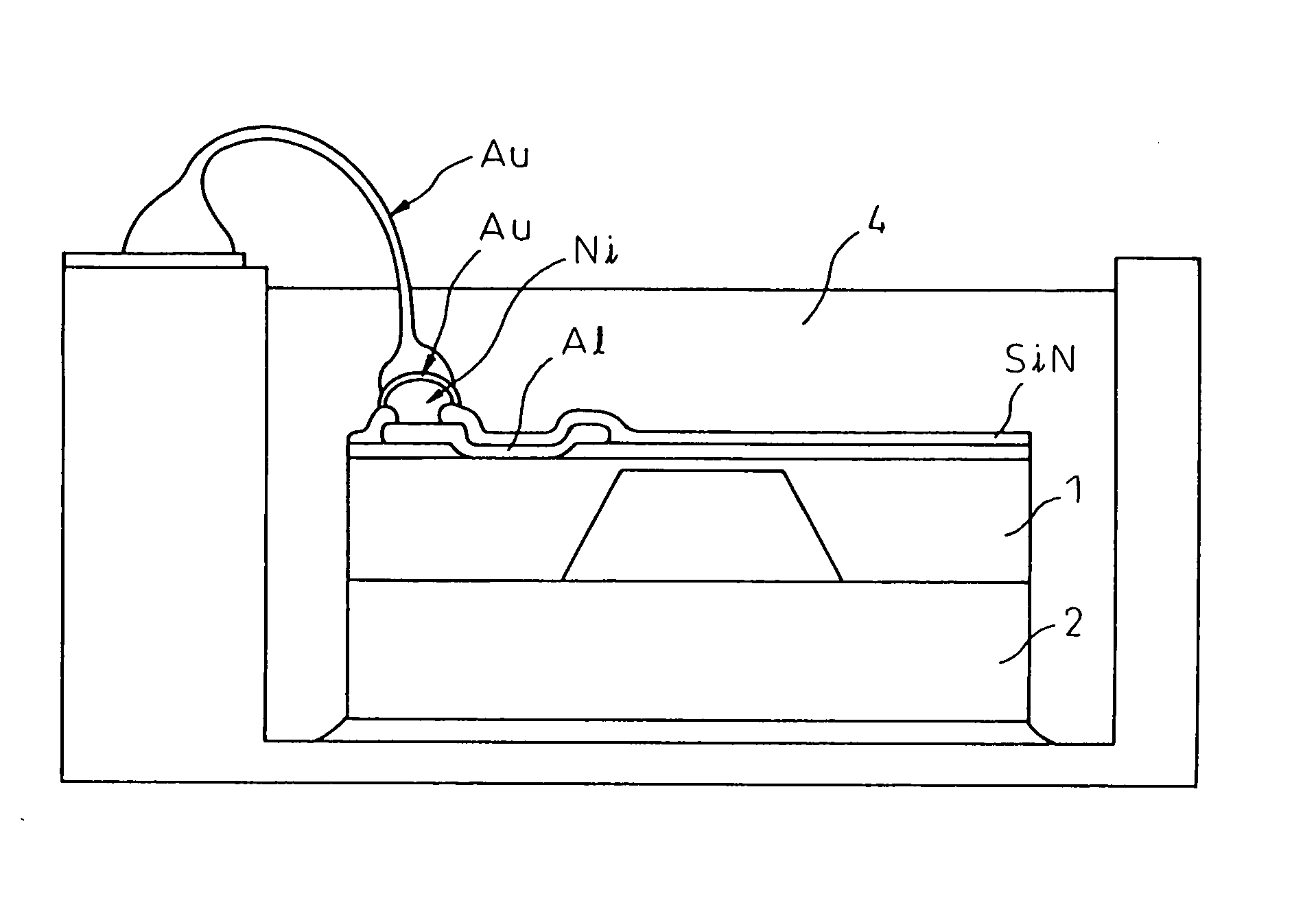
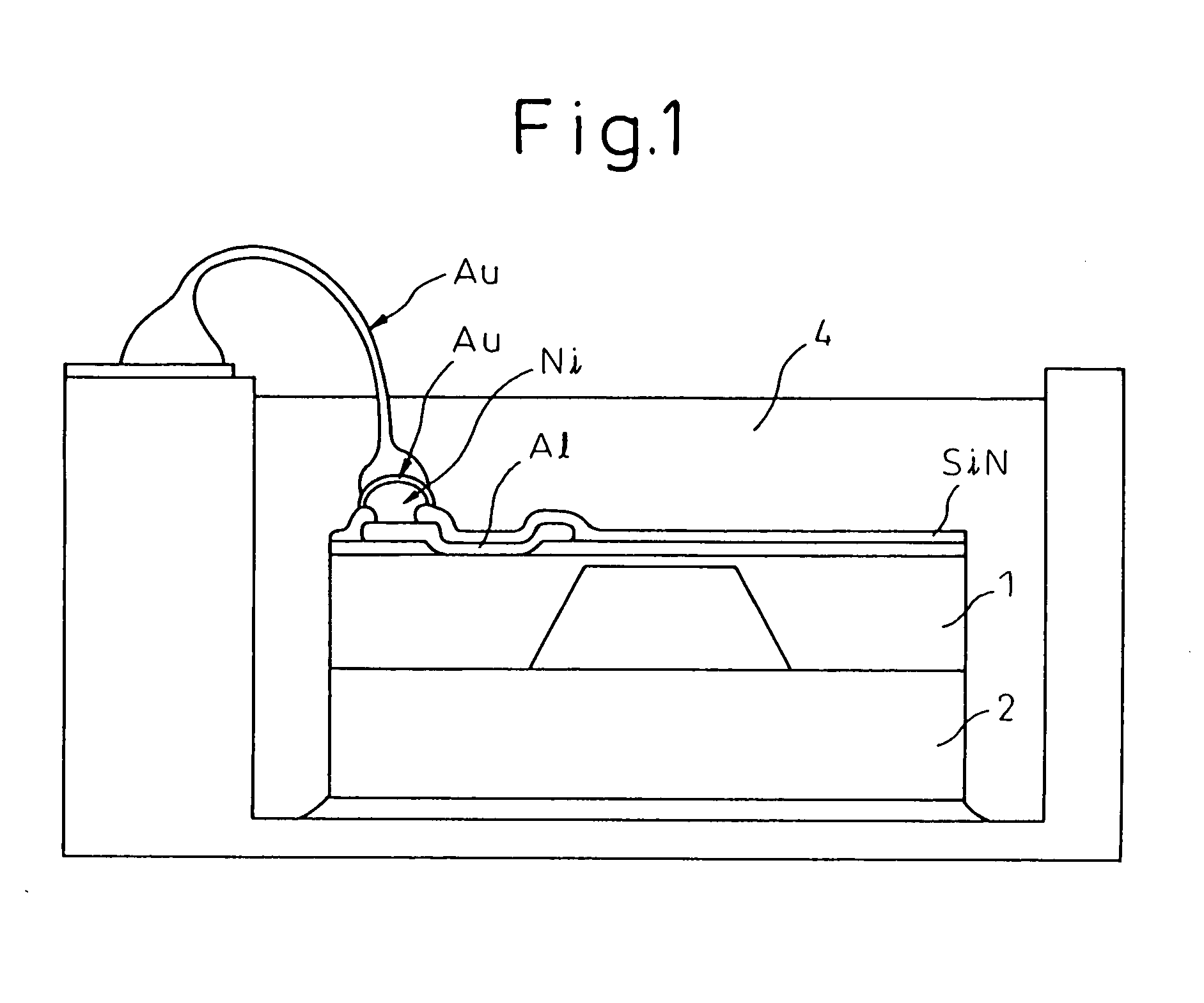
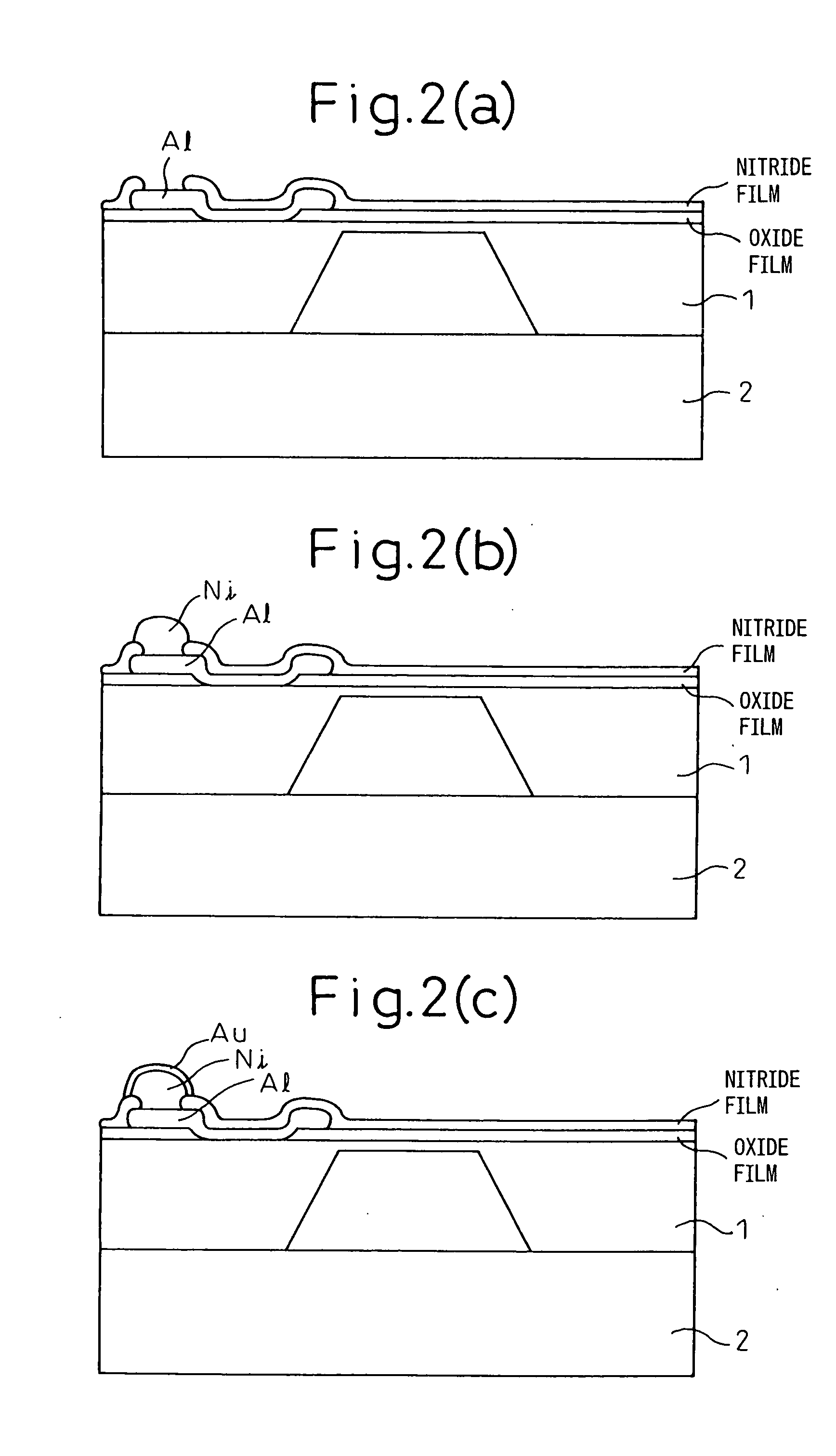
[0025] A semiconductor type sensor according to the invention has, in a semiconductor substrate such as wafer, a structural portion for detecting the physical quantity or the chemical component of a corrosive medium and an electric quantity conversion element, and has pads which are the output terminals for sending the detected electric signals to an external unit, wherein the pads are protected with a precious metal. The material forming pads is, preferably, aluminum. Usually, a glass substrate is arranged on the back surface of the semiconductor substrate. The precious metal used for protecting the pads in the present invention may be a single film of Au, Pt or Pd, or a composite film thereof. The precious metal is desirably obtained by non-electrolytically plating Ni / Au, Cu / Au, Ni / Pt or Ni / Pd and, particularly preferably, Ni / Au, successively, using a liquid not containing cyanide ions. The non-electrolytic plating is effected relying on the plating method of the invention that wi...
PUM
| Property | Measurement | Unit |
|---|---|---|
| Pressure | aaaaa | aaaaa |
| Electrical resistance | aaaaa | aaaaa |
| Electric properties | aaaaa | aaaaa |
Abstract
Description
Claims
Application Information
 - R&D Engineer
- R&D Manager
- IP Professional
- Industry Leading Data Capabilities
- Powerful AI technology
- Patent DNA Extraction
Browse by: Latest US Patents, China's latest patents, Technical Efficacy Thesaurus, Application Domain, Technology Topic.
© 2024 PatSnap. All rights reserved.Legal|Privacy policy|Modern Slavery Act Transparency Statement|Sitemap