Multi-structured Si-fin and method of manufacture

a technology of si-fin and manufacturing method, which is applied in the direction of semiconductor devices, semiconductor/solid-state device details, electrical apparatus, etc., can solve the problems of increasing cost, more complex techniques, and approximating the practical limits of technology, so as to improve the planarity and uniformity, the effect of high material points

Inactive Publication Date: 2005-02-17
SAMSUNG ELECTRONICS CO LTD
View PDF18 Cites 122 Cited by
  • Summary
  • Abstract
  • Description
  • Claims
  • Application Information

AI Technical Summary

Benefits of technology

[0021] Forming the layer of insulating material on the final silicon pattern, the insulating material having a thickness at least equal to t2, may include depositing an insulating material layer to a thickness greater than t1+t2 and removing an upper portion of the insulating material layer to expose an upper surface of the intermediate silicon pattern and an upper surface of the spacer structures. A variety of conventional techniques may be used to remove the upper portions of the insulating material including etch back and chemical-mechanical planarization (CMP) to remove the “high” points of material from a wafer to improve the planarity and uniformity for subsequent processing. Exposing at least a portion of the sidewalls of the upper silicon pattern may include removing at least an upper portion of the nitride included in the spacer structures and removing at least an upper portion of the oxide included in the spacer structures.

Problems solved by technology

Conventional bulk-MOS techniques and designs as illustrated in FIG. 1A, are, however, approaching the practical limits of the technology and are giving rise to more complex techniques in order to control the short-channel effects and obtain useable channel lengths of 100 nm and below.
These more complex techniques, however, tend to both increase the cost and decrease the yield of the resulting devices, making them less practical for general semiconductor manufacturing.
These processes, however, become increasingly difficult to control as the channel length design drops below about 100 nm.
Indeed, conventional bulk-MOS devices and technology, when pushed to achieve smaller critical dimensions, tend to exhibit undesirable channel mobility, subthreshold voltage instability, junction leakage, junction capacitance and current depletion.
Similarly, the ultra-thin body transistors are considerable more expensive that the conventional bulk-MOS devices to produce and, although providing improved performance in some areas, tend to exhibit characteristic electrical variations such as floating body and heat transfer effects and have current limitations imposed by the body thickness.
Double-gate devices, by controlling the junction from two sides, tend to exhibit improved leakage performance, but generally necessitate the use of a complicated manufacturing process that both increases the expense and lowers the yield.
FinFETs formed in this manner, however, may remain expensive to produce, limit the degree of integration that may be achieved and suffer from variable electrical performance and / or reduced yield.
FinFETs formed in this manner, however, may result in mechanical strain and / or defects at the boundary between the fin material and the isolation oxide that will tend to increase the leakage and degrade device performance and increase the difficulty of obtaining uniform filling of the spaces between adjacent fin structures.

Method used


Image

  • Multi-structured Si-fin and method of manufacture
  • Multi-structured Si-fin and method of manufacture
  • Multi-structured Si-fin and method of manufacture

Examples


Embodiment Construction

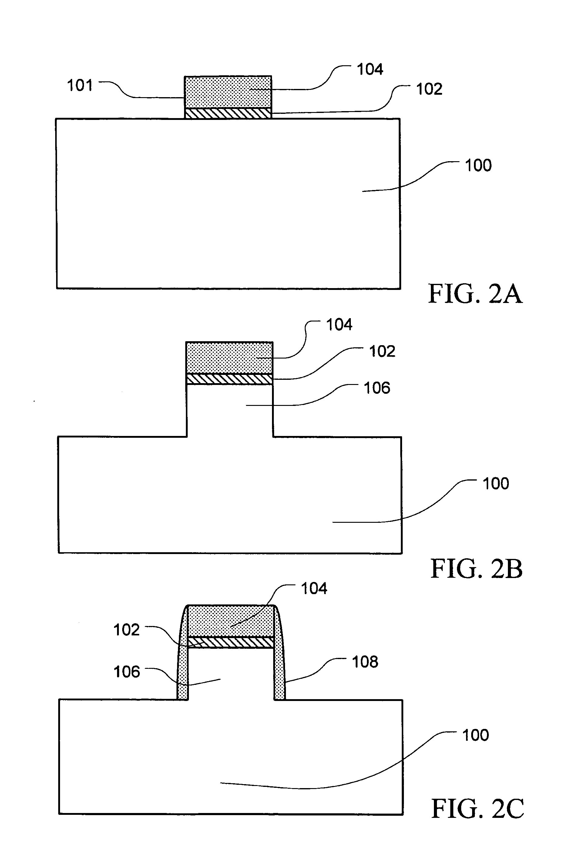
[0035] As illustrated in FIG. 2A, an exemplary method for manufacturing FinFET devices incorporating the exemplary fin configuration starts with a semiconductor substrate 100, such as silicon. The substrate utilized may be selected from a range of substrate configurations including, for example, wafers cut from Czochralski (CZ) or Float Zone (FZ) prepared single crystal bulk silicon substrates and modified substrates including, for example, substrates incorporating one or more features such as epitaxial layers, buried insulating layers or doped regions selected to provide the desired structural and performance characteristics in the completed device. An etch mask pattern 101, typically including a buffer layer 102, such as 50-200 Å of silicon dioxide, formed directly on the substrate 100 and an upper layer 104, such as 500-1000 Å of silicon nitride, formed on the buffer layer may then be formed by patterning and etching the layer(s) using conventional photolithographic and dry and / o...


PUM


Abstract

Disclosed is a semiconductor fin construction useful in FinFET devices that incorporates an upper region and a lower region with wherein the upper region is formed with substantially vertical sidewalls and the lower region is formed with inclined sidewalls to produce a wider base portion. The disclosed semiconductor fin construction will also typically include a horizontal step region at the interface between the upper region and the lower region. Also disclosed are a series of methods of manufacturing semiconductor devices incorporating semiconductor fins having this dual construction and incorporating various combinations of insulating materials such as silicon dioxide and / or silicon nitride for forming shallow trench isolation (STI) structures between adjacent semiconductor fins.

Description

CROSS-REFERENCE TO RELATED APPLICATIONS [0001] This U.S. nonprovisional patent application claims priority under 35 U.S.C. § 119 of Korean Patent Application 2003-56636 filed on Aug. 14, 2003, the entire contents of which are hereby incorporated herein by reference. BACKGROUND OF THE INVENTION [0002] 1. Field of the Invention [0003] The invention relates to an improved Si-fin structure, semiconductor devices incorporating such Si-fin structures, methods of manufacturing such improved Si-fin structures and semiconductor manufacturing processes that incorporate such manufacturing methods. [0004] 2. Description of the Prior Art [0005] Over the past 30 years, silicon-based integrated circuits and, in particular, metal-oxide-semiconductor (MOS) devices such as field effect transistors (FET or MOSFET) have consistently delivered greater speed, increased integration density and improved functionality while simultaneously reducing the cost per operation of the improved semiconductor devices...

Claims


Application Information

Patent Timeline
Patent Type & Authority Applications(United States)
IPC IPC(8): H01L21/335H01L21/265H01L21/336H01L21/8234H01L27/108H01L29/786
CPCH01L21/26513H01L21/26586H01L21/266H01L29/7851H01L21/823437H01L29/66795H01L21/823412H01L21/18
Inventor LEE, DEOK HYUNGLEE, BYEONG CHANJUNG, IN SOOSON, YONG HOONCHOI, SIYOUNGKIM, TAEK JUNG
Owner SAMSUNG ELECTRONICS CO LTD
Why Eureka
Try Eureka