Programmable eraseless memory

a technology of eraseless memory and programmable circuits, applied in the direction of digital storage, semiconductor/solid-state device details, instruments, etc., can solve the problems of complex programming and erase circuitry, complex programming and sensing technologies, etc., and achieve the effect of easy manufacturing

Inactive Publication Date: 2005-02-17
MACRONIX INT CO LTD
View PDF28 Cites 29 Cited by
  • Summary
  • Abstract
  • Description
  • Claims
  • Application Information

AI Technical Summary

Benefits of technology

[0014] The progressive breakdown phenomenon is referred to as “soft breakdown” in the Hosoi, et al., article, and as breakdown evolution “in a progressive way,” in the Wang, et al. article. The progressive breakdown characteristic of ultra-thin oxide has been characterized by a “degradation rate” which depends on stress voltage, oxide thickness, substrate doping, area and channel length in the Linder, et al., article. According to the present invention, the progressive breakdown phenomenon is applied to establish programmable resistance values in simple memory cell structures. Resulting structures are compact, can be manufactured easily with standard CMOS processes, and can be operated at low voltages.
[0042] The present invention allows for resetting data stored in memory array, where data in the memory array is stored by setting a property of memory cells in the array above or below a reference level to indicate a data value, by simply changing the reference level. The term “reset” in this context means to set all cells to a common value, usually “0” for a one bit cell, or “00” for a two bit cell, and so on. This approach to reset enables programming the array multiple times to store one or more bits per cell. The process according to this embodiment of the invention involves first resetting the memory array by changing the reference level for a single bit cell, or the set of reference levels for a multiple bit cell, so that all memory cells in the array have the sensed property lying at a level that is one of above and below the new reference level, or set of reference levels. After resetting by changing the reference, the array can be re-programmed by applying stress to selected cells as described above, using the new reference or set of references. Accordingly, a reset is executed without an “erase” operation designed to change the property of the memory cells being sensed by applying stress to the memory cells. In this sense, the method of programming according to the present invention can be characterized as “eraseless.”

Problems solved by technology

Memory technologies based upon floating gates like standard EEPROM, or charge trapping layers like oxide-nitride-oxide memory cells, are typically programmable many times. However, these technologies require complex programming and erasing circuitry, and employ complex charge pump techniques to achieve the voltages required for programming and erasing.
Also, when storing more than one bit of data per memory cell, complex programming and sensing technologies are required.
Finally, with respect to these types of flash memory, manufacturing steps needed to form the memory cells often include expensive steps not normally required for forming standard logic circuitry, such as CMOS logic, on the same integrated circuit.
Although the de Graaf, et al., structure is compact and easy to manufacture, it allows only one-time programming, and requires high-voltage operation.

Method used


Image

  • Programmable eraseless memory
  • Programmable eraseless memory
  • Programmable eraseless memory

Examples


Embodiment Construction

[0083] A detailed description of embodiments of the present invention is provided with reference to FIGS. 1-36.

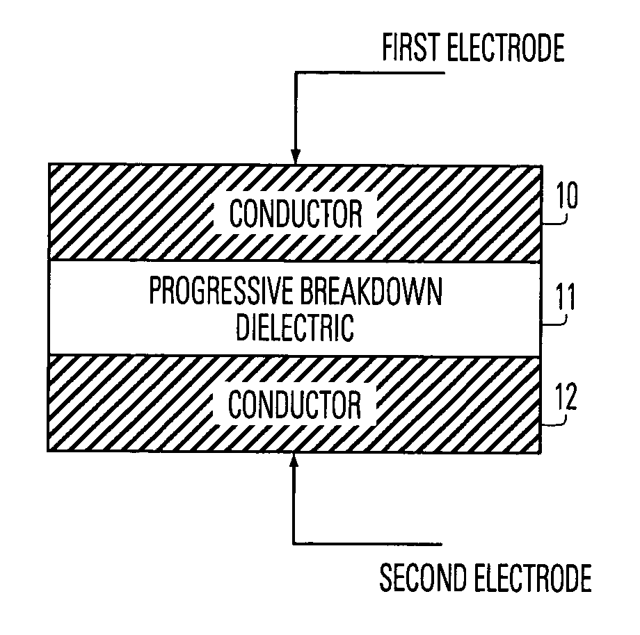
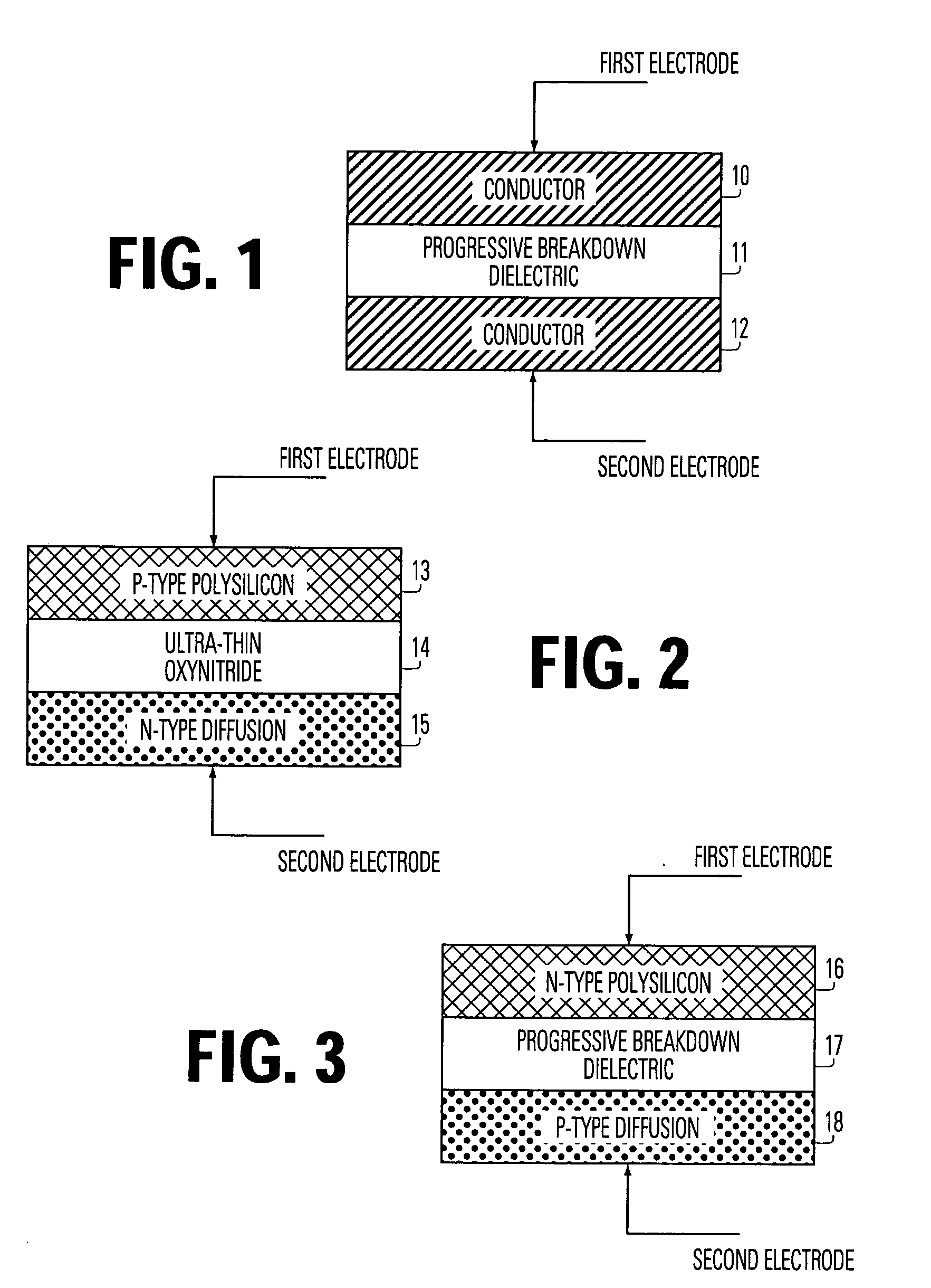
[0084]FIGS. 1-3 illustrate basic memory cell structures according to the present invention. As shown in FIG. 1, a memory cell comprises a conductor 10, a progressive breakdown dielectric film 11, and a conductor 12. The conductor 10 acts as a first electrode. The conductor 12 acts as a second electrode. The dielectric film 11 comprises a material having a thickness or other structural feature, characterized by a property subject to progressive change in response to stress. Representative dielectrics which exhibit the progressive breakdown characteristic causing progressive change in resistance, include ultra-thin oxides, such as oxynitride having a thickness of less than 20 Angstroms, and more preferably about 15 Angstroms or less.

[0085] One way in which oxynitride can be formed comprises using standard thermal silicon dioxide growth processes, along with or followed by n...


PUM


Abstract

An electrically programmable non-volatile memory cell comprises a first electrode, a second electrode and an inter-electrode layer, such as ultra-thin oxide, between the first and second electrodes which is characterized by progressive change in resistance in response to program stress of relatively low voltages. A programmable resistance representing stored data is established by stressing the inter-electrode layer between the electrodes. Embodiments of the memory cell are adapted to store multiple bits of data per cell and / or adapted for programming more than one time without an erase process.

Description

REFERENCE TO RELATED APPLICATION [0001] The present application claims the benefit of Provisional U.S. Patent Application No. 60 / ______, entitled PROGRAMMABLE RESISTOR ERASELESS MEMORY, invented by Yeh, et al., and filed on 21 Jul. 2003 (converted application Ser. No. 10 / ______ from non-provisional status to provisional status). [0002] The present application is related to U.S. patent application No. 10 / ______, entitled METHOD FOR PROGRAMMING PROGRAMMABLE ERASELESS MEMORY, invented by Yeh, et al., and filed on the same day as the present application. [0003] The present application is related to U.S. patent application Ser. No. 10 / ______, entitled METHOD FOR MANUFACTURING A PROGRAMMABLE ERASELESS MEMORY, invented by Yeh, et al., and filed on the same day as the present application.BACKGROUND OF THE INVENTION [0004] 1. Field of the Invention [0005] The present invention relates to electrically programmable, non-volatile memory and integrated circuits including such memory, and more pa...

Claims


Application Information

Patent Timeline
Patent Type & Authority Applications(United States)
IPC IPC(8): G11C16/04G11C11/56H01L27/10
CPCG11C11/5692
Inventor YEH, CHIH CHIEHLAI, HAN CHAOTSAI, WEN JERLU, TAO CHENGLU, CHIH YUAN
Owner MACRONIX INT CO LTD
Why Eureka
Try Eureka