Double-sided, edge-mounted stripline signal processing modules and modular network

a signal processing module and modular network technology, applied in the field of stripline signal processing systems, can solve the problems of increasing the cost of the circuit, reducing the physical ruggedness of the circuit, and the theoretical lossless loss of the ideal non-absorbing circuit between the ports, so as to reduce the cost, reduce the size, and reduce the cost

Inactive Publication Date: 2005-02-17
ANDREW CORP
View PDF33 Cites 30 Cited by
  • Summary
  • Abstract
  • Description
  • Claims
  • Application Information

AI Technical Summary

Benefits of technology

[0022] The results is a compact, edge-mounted, double-sided, modular signal processing PC board design that is well suited to assembling higher-order circuits from complexes of lower-order, edge-mounted modules. This architecture may be used to construct hybrid matrix amplifiers (HMAs) and beam forming networks for multi-beam antenna systems that exhibit many advantages over prior HMA and beam forming networks including decreased size, decreased cost, standardization of module design, scalability, repeatability of manufactured products, ease of construction, and ease of repair and maintenance. Circuit configurations implemented in this manner can also be readily configured to exhibit low noise generation, low power and signal losses, and rugged physical construction.

Problems solved by technology

In addition, the input and output impedances of the orthogonal circuit are typically matched across connecting junctions or ports so that the ideal non-absorbing circuit is theoretically lossless for signal flow between ports.
The drawback in using this construction paradigm is that beam forming networks using hybrid junctions are often characterized by crossover points in which stripline segments must pass by each other physically without interfering with each other electrically.
On a PC board, the need for crossovers presents a design challenge because the stripline segments must remain physically separated from each other to avoid electrical interconnection (if the stripline segments physically touch each other) or radiating interference or cross-talk (if the stripline segments come too close together without physically touching each other).
Each of these designs increases the cost of the circuit, reduces the physical ruggedness of the circuit, and has the potential to increase noise generation and RF signal loss, particularly at junctions between different types of transmission media segments.
More importantly, these somewhat clumsy solutions to the crossover problem greatly complicate the manufacturing process because the entire circuit cannot be arranged on a single PC board using stripline transmission media segments formed into the PC board that can then be manufactured through a conventional etching techniques and processes.
Although this type of crossover can be implemented on a single flat PC board without physical trace jumps, it occupies a relatively large section of PC board space.
Because the crossover is a basic building block that is repeated many times in creating a higher-level beam forming network, the significant board size required to implement the zero-dB crossover quickly multiplies into an overly large and expensive PC board as the complexity of the bream forming network increases.
Further, designing each stripline segment to have a precisely determined phase characteristic at RF and microwave operational frequencies also requires the stripline circuit to be physically arranged on the printed circuit board in a manner that consumes a relatively large amount of planar board space.
Materials with substantially higher dielectric constant values can be substantially more expensive, can have higher RF signal losses, and can have RF power handling limitations that are a lower value due to reduced stripline trace width values.
The physical size of the PC board starts to become unwieldy and expensive as the number of hybrid junction elements increases beyond the eight to 16 element level.
Arranging a stripline signal processing circuit on a planar PC board in the conventional manner for these circuits would result on a very large PC board that would be very expensive to manufacture and install in a secure manner.
Nor does it teach or suggest mechanisms for minimizing the PC board space required to implement higher-order analog signal processing circuits.

Method used


Image

  • Double-sided, edge-mounted stripline signal processing modules and modular network
  • Double-sided, edge-mounted stripline signal processing modules and modular network
  • Double-sided, edge-mounted stripline signal processing modules and modular network

Examples


Embodiment Construction

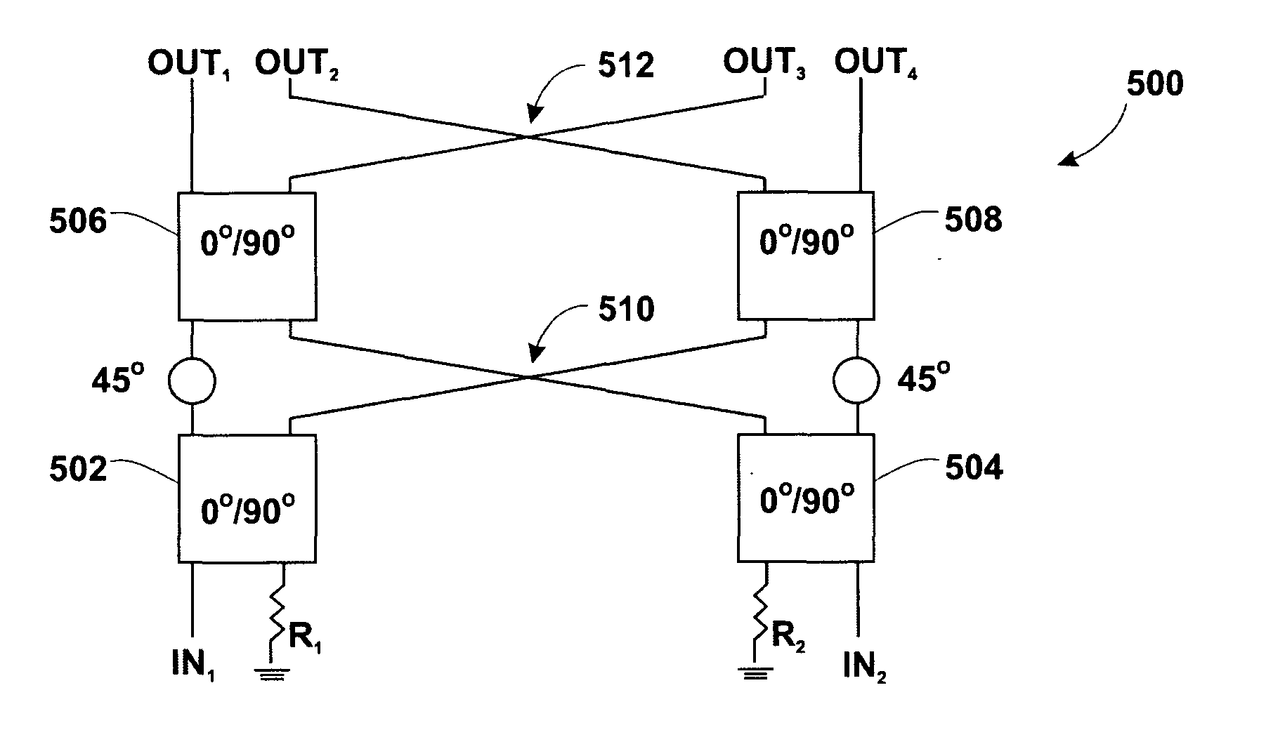
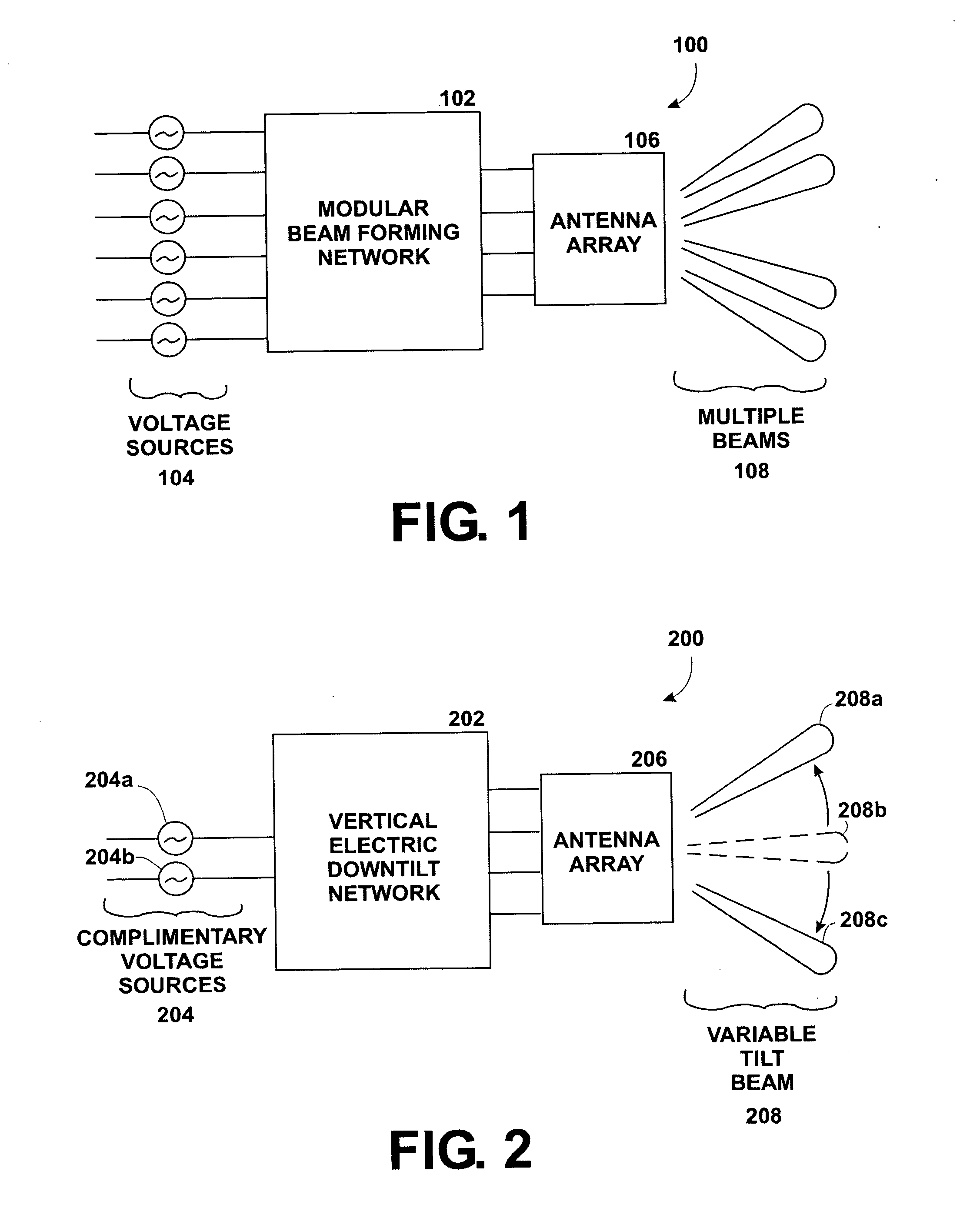
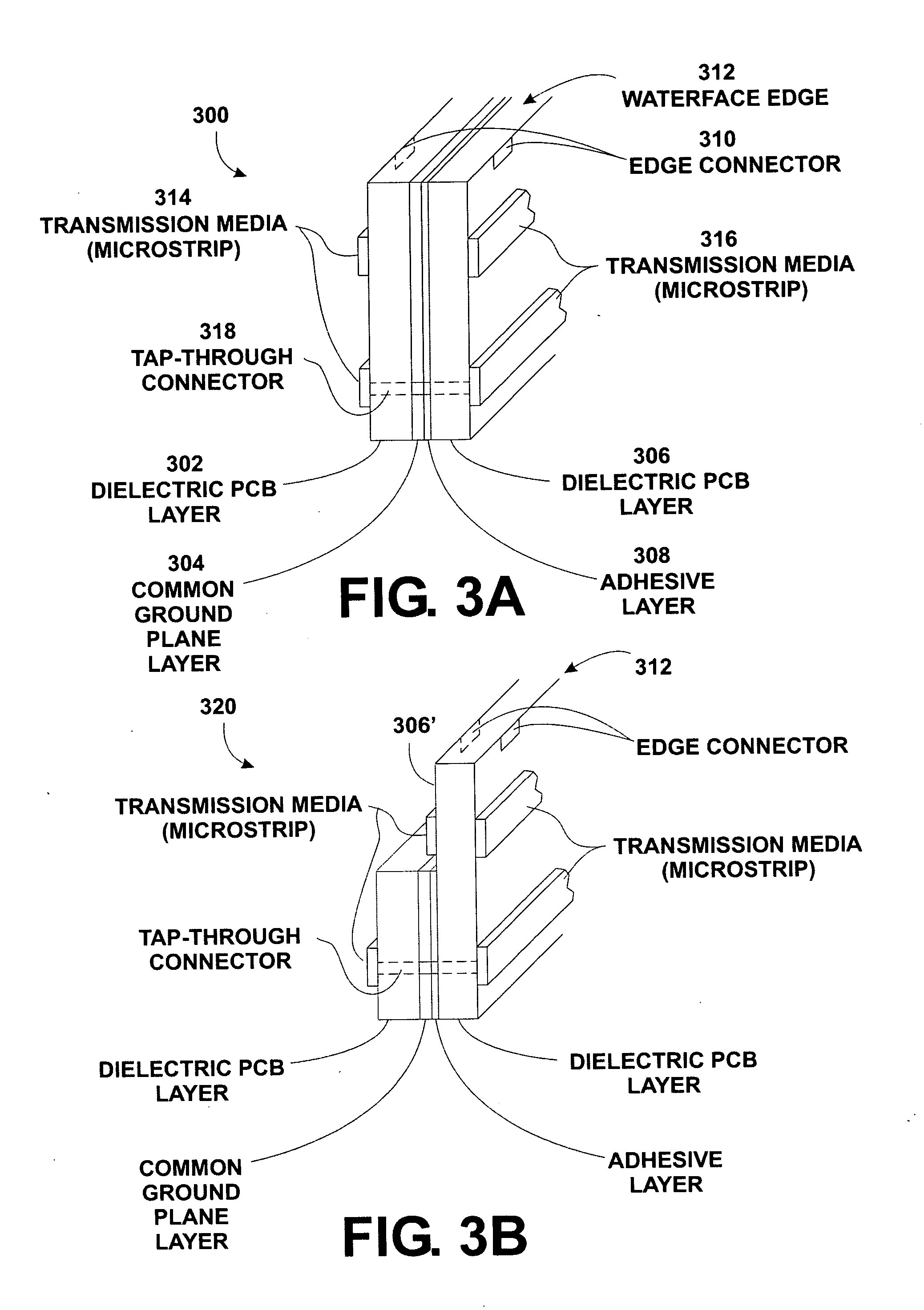
[0062] The present invention relates to a class of double-sided, edge-mounted printed circuit (PC) modules and an associated modular network architecture for constructing stripline signal processing networks including high-power analog amplifiers and beam forming networks for use in multi-beam antenna systems. The stripline signal processing networks are characterized by network elements constructed from defined-length segments of stripline configured to exhibit precisely determined phase and impedance characteristics. These circuits may also include conventional passive “lumped” electrical elements, such as resistors, capacitors and inductors; non-linear circuit elements such as diodes; and active electrical elements, such as amplifiers and transistors.

[0063] The stripline segments are typically constructed from conductive stripline, such as tin-covered copper traces, carried on a dielectric PC board substrate constructed from, for example, PTFE Teflon® laminate impregnated with g...


PUM


Abstract

A class of modular, double-sided, edge-mounted printed circuit (PC) board modules and an associated modular network architecture for constructing stripline signal processing networks including high-power analog amplifiers and beam forming networks for driving multi-beam antenna systems. The stripline signal processing networks are characterized by network elements constructed from defined-length segments of transmission media configured to exhibit precisely determined phase and impedance characteristics. These circuits may also include conventional passive “lumped” electrical elements, such as resistors, capacitors and inductors; non-linear circuit elements such as diodes; and active electrical elements, such as amplifiers and transistors.

Description

TECHNICAL FIELD [0001] The present invention relates to stripline signal processing systems for radio and microwave frequency applications and, more particularly, relates to a class of double-sided, edge-mounted printed circuit (PC) modules and an associated modular network architecture for constructing stripline signal processing networks including high-power analog amplifiers and beam forming networks for shaped beam and / or multi-beam antenna systems. BACKGROUND OF THE INVENTION [0002] Stripline signal processing circuits can be used to implement a variety of analog signal operations on electromagnetic energy propagating within the circuit at radio frequency (RF) and microwave transmission frequencies. Generally stated, a stripline signal processing circuit, as that term is used in this specification, is a circuit that includes one or more transmission media segments of specified lengths and impedance characteristics, which are typically interconnected into a network, and which ex...

Claims


Application Information

Patent Timeline
Patent Type & Authority Applications(United States)
IPC IPC(8): H01Q21/00H05K1/02H05K1/11
CPCH01Q21/0025H01Q21/0075H01Q21/0087H05K1/0237H05K1/117H01L2924/0002H05K2201/0379H05K2201/09845H01L2924/00H01P3/08H01L23/66H01K1/02
Inventor CARSON, JAMES CRAWFORD
Owner ANDREW CORP
Why Eureka
Try Eureka