Failure analysis vehicle for yield enhancement with self test at speed burnin capability for reliability testing

a failure analysis and reliability testing technology, applied in the direction of testing/monitoring control systems, instruments, semiconductor/solid-state device testing/measurement, etc., can solve the problems of failure analysis of some integrated circuits that may be very time-consuming, and may take days or even weeks to isola

Inactive Publication Date: 2005-02-24
BELL SEMICON LLC
View PDF2 Cites 2 Cited by
  • Summary
  • Abstract
  • Description
  • Claims
  • Application Information

AI Technical Summary

Benefits of technology

[0022] The advantages of the present invention are that an integrated circuit may be manufactured that stresses many of the design limits of the manufacturing process. Further, the full and unfettered test access to many of the signal traces allows an engineer or technician ...

Problems solved by technology

After the first production of a new integrated circuit design, there is generally a period of failure analysis as the design and manufacturing processes are adjusted to produce a successful product.
The root cause failure analysis of some integrated circuits may be very time consuming, sometimes consuming days or even weeks to isolate a single fault on a single chip.
In addition, destructive tests, such as etching and lapping, may...

Method used


Image

  • Failure analysis vehicle for yield enhancement with self test at speed burnin capability for reliability testing
  • Failure analysis vehicle for yield enhancement with self test at speed burnin capability for reliability testing
  • Failure analysis vehicle for yield enhancement with self test at speed burnin capability for reliability testing

Examples


embodiment 100

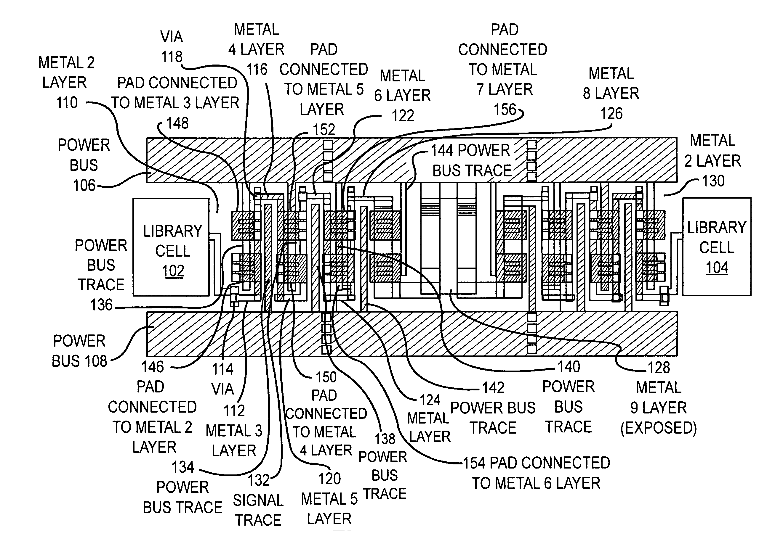
[0039]FIG. 1 illustrates an embodiment 100 of a staircase interconnect between two library cells 102 and 104 of an integrated circuit. Two power busses, 106 and 108, supply power to the cells, 102 and 104. The signal trace leaving cell 102 begins on the metal 2 layer 110 and transfers to the metal 3 layer 112 with the via 114. The signal trace then transfers to the metal 4 layer 116 with the via 118. The signal trace continues to metal 5 layer 120, metal 6 layer 122, metal 7 layer 124, and metal 8 layer 126 in a serpentine fashion. The signal trace continues to metal 9 layer 128. The serpentine pattern is repeated in a similar fashion from metal 9 layer 128 to metal 2 layer 130 and into the second library cell 104.

[0040] Within each serpentine pattern, a trace from a power bus is placed in close proximity. For example, on the metal 4 layer 116, the signal trace 132 is in close proximity to the trace 134 that is connected to the power bus 108. In a similar fashion, power bus traces 1...

embodiment 300

[0051]FIG. 3 illustrates an embodiment 300 for a unit delay schematic. The data in 302 passes through a circuit to the data out 304. The circuit comprises a buffer 306, a staircase of vias 308, a NOR gate 310, a second staircase 312, a NAND gate 314, a third staircase 316, an inverter 318, and a fourth staircase 319. The power bus comprises VDD 320 and VCC 322, which are connected to the NOR 310 and NAND 314 so that a positive signal is transmitted through the circuit. The time that is taken for the signal to propagate through the circuit can be known.

[0052] In a typical embodiment, the circuit 300 may be connected end to end many times, possibly hundreds or thousands of times in a single integrated circuit. The unit delay circuit 300 may be used in several different useful embodiments.

embodiment 400

[0053]FIG. 4 illustrates an embodiment 400 of a physical layout of the unit delay cell illustrated in FIG. 3. The circuit comprises the buffer 406, a first staircase 408, a NOR gate 410, a second staircase 412, a NAND gate 414, a third staircase 416, an inverter 418, and a fourth staircase 419. The VDD 420 and VCC 422 power busses are also shown.

[0054] The cells may be arranged such that the power busses are aligned. This arrangement allows easy mechanical cross sectioning of the circuits to inspect problem areas. In the cross sections, known good traces may be compared to suspected bad traces because of the repeating pattern of the embodiment 400.


PUM


Abstract

A test vehicle for evaluating a manufacturing process for integrated circuits that uses a more space efficient layout of library driving cells arranged to produce circuits that exercise many interconnections that may be designed at the minimum design parameters of a manufacturing process. The cells can be configured to operate as ring oscillators increasing the effective circuit frequency of the test module allowing higher frequency circuit testing, and shortening the time it takes to perform life cycle testing. Visibly marking cells, combined with electrically isolating error prone circuit segments makes, identifying defects much more efficient. The accessibility of many testing methods allows quick location of root cause failures, which allows improvements to be made to the manufacturing process.

Description

CROSS REFERENCE TO RELATED APPLICATIONS [0001] This application is a continuation-in-part of U.S. patent application Ser. No. 10 / 307,018 entitled “Failure Analysis Vehicle” by Richard Schultz and Steve Howard, filed Nov. 27, 2002, the entire contents of the which is hereby specifically incorporated herein by reference for all it discloses and teaches.BACKGROUND OF THE INVENTION [0002] a. Field of the Invention [0003] The present invention pertains to integrated circuit manufacturing and specifically to test samples used to qualify a new manufacturing process. [0004] b. Description of the Background [0005] In the development of a new manufacturing process for integrated circuits, certain design rules are created that define the capabilities of the process. A designer begins the design of new integrated circuits at the same time as the manufacturing capability is being developed. The concurrency of new process development and product design places great importance on the ability of th...

Claims


Application Information

Patent Timeline
IPC IPC(8): G01R31/26G05B23/02G06F19/00H01L23/58H01L29/73H01L29/74
CPCG01R31/2884G05B23/0256G01R33/18G01R31/3016
Inventor SCHULTZ, RICHARDSCHMIDT, MICHAEL
Owner BELL SEMICON LLC
Why Eureka
Try Eureka