Semiconductor memory device and portable electronic apparatus

a memory device and semiconductor technology, applied in the direction of digital storage, solid-state devices, instruments, etc., can solve the problems of disturbing the reduction in the size of the memory cell, the difficulty of effectively reducing the thickness of the insulating film, etc., to achieve uniform picture quality, improve operation speed, and suppress manufacturing costs

Inactive Publication Date: 2005-02-24
TELEMANN FUND NINE LIMITED LIABILITY
View PDF4 Cites 8 Cited by
  • Summary
  • Abstract
  • Description
  • Claims
  • Application Information

AI Technical Summary

Benefits of technology

[0015] In the semiconductor memory device according to the present invention, the memory cell includes a gate electrode formed over a semiconductor layer via a gate insulating film, a channel region disposed below the gate electrode, diffusion regions disposed on both sides of the channel region and having a conductive type opposite to that of the channel region, and memory functional elements formed on both sides of the gate electrode and having the function of retaining charges. A memory function of the memory functional element and a transistor operation function of the gate insulating film are separated from each other. Consequently, it is easy to suppress the short channel effect by thinning the gate insulating film while maintaining the sufficient memory function. Further, a value of current flowing between the diffusion regions changes by rewriting more largely than that in the case of an EEPROM. Therefore, it facilitates discrimination between the programming state and the erasing state of the semiconductor memory device.
[0016] Further, the memory cell in the semiconductor memory device according to the present invention can be formed by a process which is very compatible with a normal transistor forming process on the basis of the configuration. Therefore, as compared with the case of using a conventional flash memory as a nonvolatile memory cell and configuring the semiconductor memory device having a peripheral circuit which is usually made by a transistor, the number of masks and the number of processes can be dramatically reduced. Consequently, the yield in manufacturing of the semiconductor memory device having both the memory cell and the peripheral circuit can be improved. Accordingly, the manufacturing cost is reduced and a very-reliable, cheap semiconductor memory device can be obtained.
[0017] Further, the present invention can provide a semiconductor memory device having the high degree of freedom in use and application and realizing largely improved throughput of operations to be processed as a whole. Overhead of a microprocessor using the semiconductor memory device according to the present invention can be minimized, and there is no fear of erroneous operations and over-erasure of a memory cell array. Components of the semiconductor memory device according to the present invention cooperate with each other, thereby providing all of functions for operations of the memory cell array.
[0018] The user interface circuit of the semiconductor memory device according to the present invention receives an address, a command and data information from an external user such as a microprocessor via a bus and issues a command to the array control circuit. The array control circuit executes an erasing / programming operation specified by the command issued by the user interface circuit. The array control circuit controls voltages (program voltage, erase voltage and the like) for executing the memory cell array operation and a specified operation independently of the user interface circuit. As a result, a very high degree of freedom is achieved, and the user interface circuit can accept various user commands and can control a sequence of a command transferred to the array control circuit so as to be executed. Commands can be pipeline-processed, so that the maximum throughput can be provided. Further, the array control circuit executes an operation on the basis of the code stored in the program memory. Therefore, by simply correcting a microcode in the program memory, a new command can be added and an existing command can be changed without changing hardware.
[0020] With such a configuration, in the case of using the semiconductor memory device of the present invention for storing information for correcting variations in display after a display panel is manufactured, uniform picture quality can be obtained in products of the displays. Moreover, the process of simultaneously forming the memory cell and the logic circuit is simple, so that the manufacturing cost can be suppressed and the operation speed can be improved by high-speed reading operation. Thus, the cheap and high-performance display and the portable electronic apparatus can be obtained.

Problems solved by technology

Consequently, it is difficult to effectively reduce the thickness of the insulating film 907 and the gate insulating film, and it disturbs reduction in the size of the memory cell.

Method used


Image

  • Semiconductor memory device and portable electronic apparatus
  • Semiconductor memory device and portable electronic apparatus
  • Semiconductor memory device and portable electronic apparatus

Examples


first embodiment

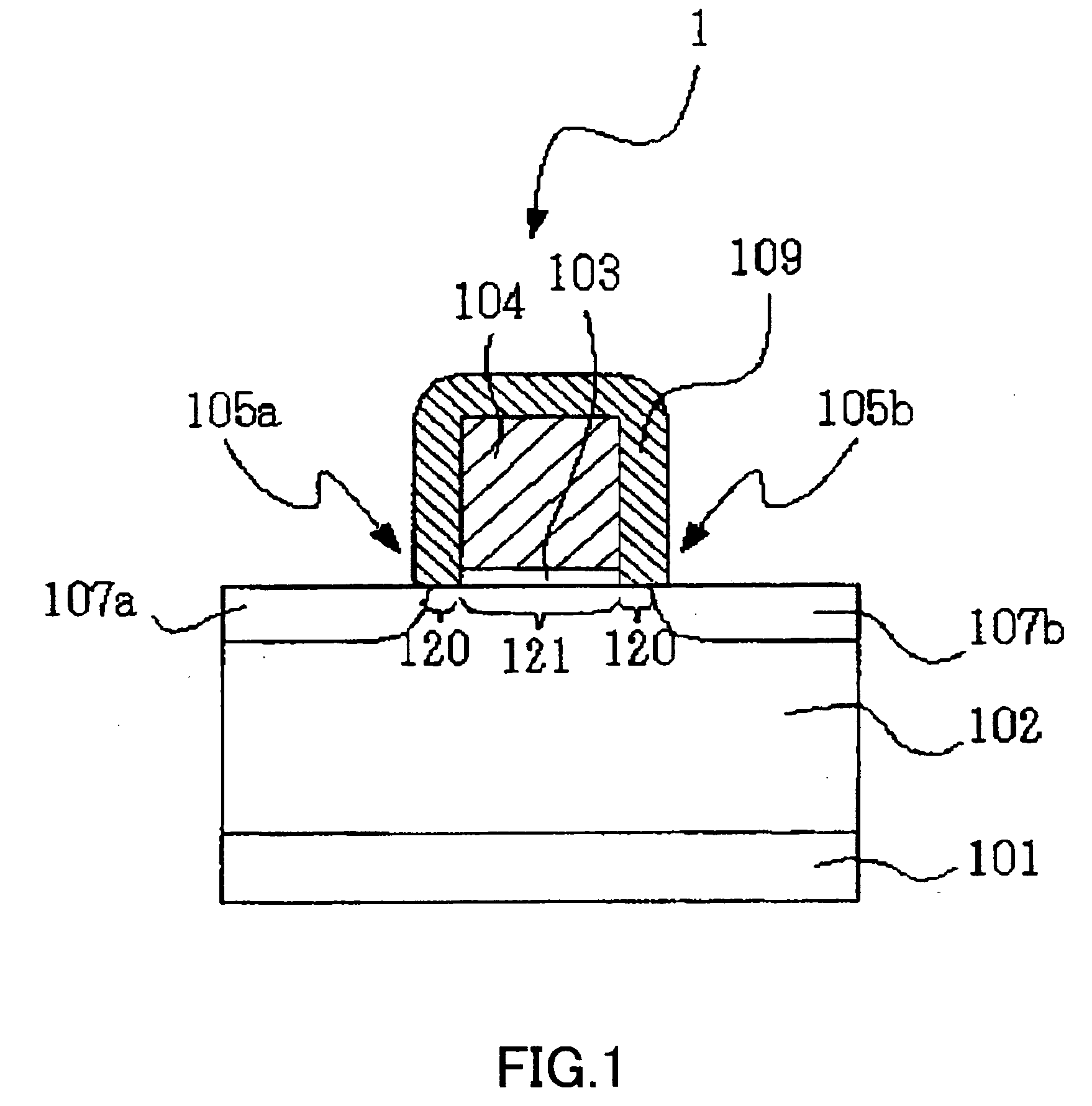
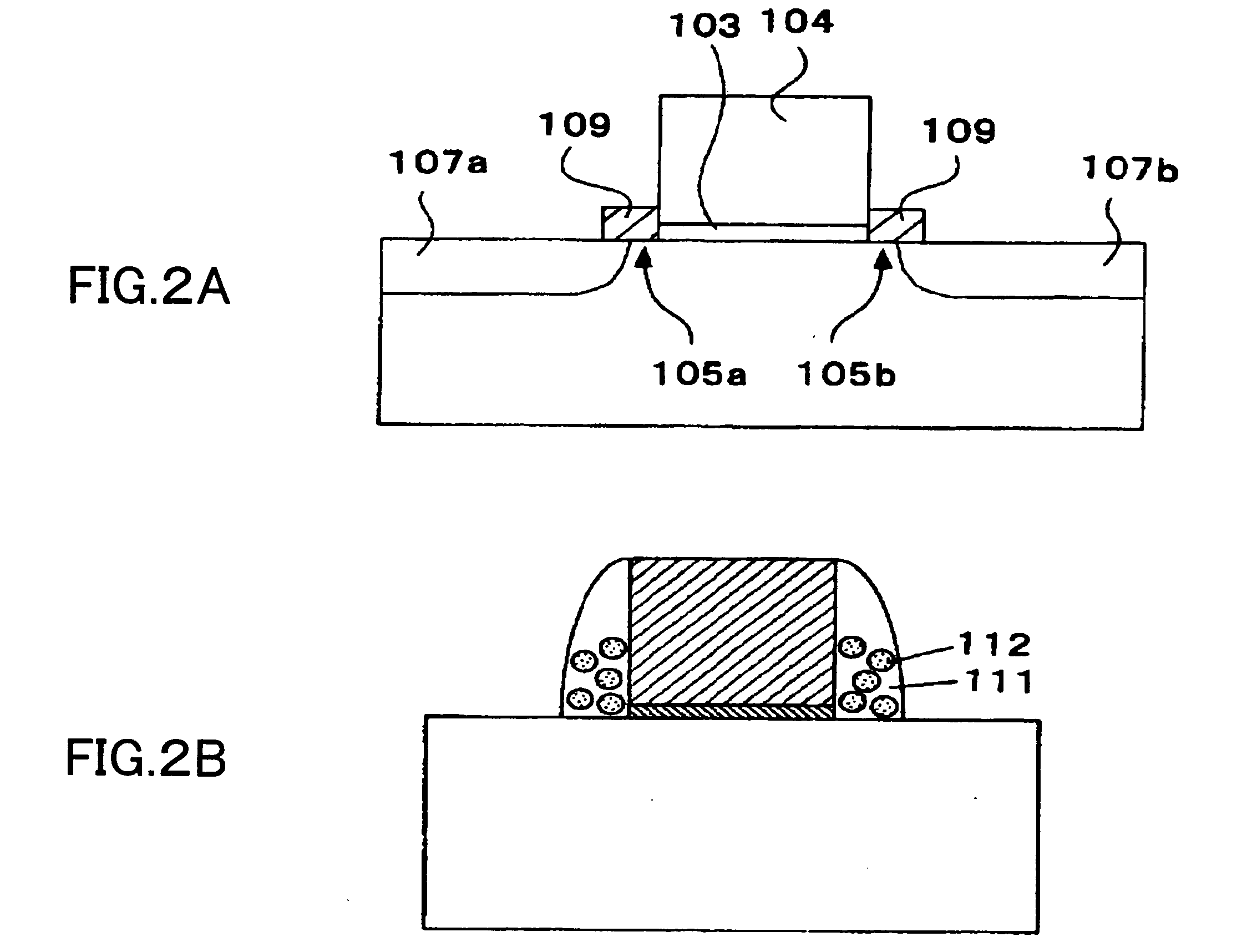
[0085] A semiconductor memory device of a first embodiment has a memory cell 1 as shown in FIG. 1.

[0086] The memory cell 1 has a gate electrode 104 formed on a P-type well region 102 formed on the surface of a semiconductor substrate 101 via a gate insulating film 103. On the top face and side faces of the gate electrode 104, a silicon nitride film 109 having a trap level of retaining charges and serving as a charge retaining film is disposed. In the silicon nitride film 109, parts of both sidewalls of the gate electrode 104 serve as memory functional elements 105a and 105b for actually retaining charges. The memory functional element refers to a part in which charges are actually accumulated by rewriting operation in the memory functional element or the charge retaining film. In the P-type well region 102 on both sides of the gate electrode 104, N-type diffusion regions 107a and 107b functioning as a source region and a drain region, respectively, are formed. Each of the diffusion...

second embodiment

[0106] A memory cell in a semiconductor memory device according to a second embodiment has a configuration substantially similar to that of the memory cell 1 of FIG. 1 except that, as shown in FIG. 8, each of memory functional elements 261 and 262 is configured by a charge retaining region (which is a charge accumulating region and may be a film having the function of retaining charges) and a region for suppressing escape of charges (or a film having the function of suppressing escape of charges).

[0107] Preferably, from the viewpoint of improving the retaining characteristic of the memory, the memory functional element includes a charge retaining film having the function of retaining charges and an insulating film. In the embodiment, a silicon nitride film 242 having a level of trapping charges is used as the charge retaining film and silicon oxide films 241 and 243 having the function of preventing escape of charges accumulated in the charge retaining film are used as the insulati...

third embodiment

[0126] The memory functional element 262 in a semiconductor memory device of a third embodiment has a shape in which, as shown in FIG. 13, the silicon nitride film 242 as the charge retaining film has an almost constant thickness and is disposed almost parallel with the surface of the gate insulating film 214 (region 281) and, further, disposed almost parallel with a side surface of the gate electrode 217 (region 282).

[0127] In the case where a positive voltage is applied to the gate electrode 217, an electric line 283 of force in the memory functional element 262 passes through the silicon nitride film 242 twice (portions corresponding to the regions 282 and 281) as shown by the arrows. When a negative voltage is applied to the gate electrode 217, the direction of the electric line of force is reversed. The dielectric constant of the silicon nitride film 242 is about 6 and the dielectric constant of the silicon oxide films 241 and 243 is about 4. Therefore, as compared with the ca...


PUM


Abstract

The present invention provides a semiconductor memory device including a memory cell array in which a plurality of memory cells are arranged, a user interface circuit including a command queue having a logic circuit for accepting commands issued by an external user and generating a program memory address, and an array control circuit having a microcontroller and a program memory for storing therein an execution code, and executing an operation on the memory cell array, wherein the memory cell includes a gate electrode formed over a semiconductor layer via a gate insulating film, a channel region disposed below the gate electrode, diffusion regions disposed on both sides of the channel region and having a conductive type opposite to that of the channel region, and memory functional elements formed on both sides of the gate electrode and having the function of retaining charges.

Description

BACKGROUND OF THE INVENTION [0001] 1. Field of the Invention [0002] The present invention relates to a semiconductor memory device, a display and a portable electronic apparatus. More specifically, the present invention relates to a semiconductor memory device in which field-effect transistors each including a memory functional element having the function of retaining charges or polarization are arranged, and to a display and a portable electronic apparatus each having such a semiconductor memory device. [0003] 2. Description of the Related Art [0004] Conventionally, a flash memory is typically used as a nonvolatile memory. [0005] In a flash memory, as shown in FIG. 29, a floating gate 902, an insulating film 907 and a word line (control gate) 903 are formed in this order on a semiconductor substrate 901 via a gate insulating film. On both sides of the floating gate 902, a source line 904 and a bit line 905 are formed by a diffusion region, thereby configuring a memory cell. A devic...

Claims


Application Information

Patent Timeline
Patent Type & Authority Applications(United States)
IPC IPC(8): G11C16/04G11C16/02G11C16/08G11C16/10G11C16/16H01L21/28H01L21/336H01L21/8234H01L21/8247H01L27/088H01L27/10H01L27/115H01L29/788H01L29/792
CPCG11C16/0475G11C16/10G11C16/16H01L29/66833H01L29/7923H01L29/40117
Inventor MATSUOKA, NOBUAKINAWAKI, MASARUMORIKAWA, YOSHINAOIWATA, HIROSHISHIBATA, AKIHIDE
Owner TELEMANN FUND NINE LIMITED LIABILITY
Why Eureka
Try Eureka