Apparatus for laser beam machining, machining mask, method for laser beam machining, method for manufacturing a semiconductor device and semiconductor device

a laser beam and machining mask technology, applied in the field of laser beam machining, can solve the problems of easy peeling, poor mechanical strength of low-k dielectric film, and peeled interlevel dielectric film, and achieve the effect of increasing adhesion strength

Inactive Publication Date: 2005-03-03
KK TOSHIBA
View PDF8 Cites 50 Cited by
  • Summary
  • Abstract
  • Description
  • Claims
  • Application Information

AI Technical Summary

Benefits of technology

[0019] A fifth aspect of the present invention inheres in a semiconductor device including a semiconductor substrate; a plurality of interlevel dielectric films deposited on a surface of the semiconductor substrate; and a diffusion barrier film deposited between the plurality of interlevel dielectric films and having a region reformed so as to increase adhesion strength between the diffusion barrier film and the interlevel dielectric films in the vicinity of a chip periphery.

Problems solved by technology

However, when dicing is performed by use of a blade on the semiconductor device having the low-k dielectric film as an interlevel dielectric film, the interlevel dielectric film is peeled off.
When the Si substrate having the multilevel film formed thereon is diced by use of a blade, peeling easily occurs, due to poor adhesion, from an interface of the SiC film, the Si3N4 film, the SiCN film or the like.
Moreover, cracks occur in the low-k dielectric film, such as the organic silicon oxide film and the porous silicon oxide film, because mechanical strength of the low-k dielectric film is poor.
However, in current laser beam machining, the ablation of the diffusion barrier film or the Si substrate provides a stress on the low-k dielectric film and cracks are generated in the low-k dielectric film.
However, the cracks formed in a direction orthogonal to the scanning direction are left in the semiconductor chips after the laser beam machining.
However, the generation of cracks in the low-k dielectric film cannot be suppressed, which leads to a problem of low reliability of a device so fabricated.
Moreover, when the Si substrate is diced by use of a blade, it is difficult to suppress generation of cracks in the Si substrate.
Consequently, the generated cracks may cause a decrease in chip strength associated with thinning of the semiconductor chips.
However, if the focal depth is increased, laser beam narrowing is limited and the laser beam machining becomes difficult.
The removal of the crushed layer by wet etching increases the loss of the effective area for the substrate and decreases production yield of the semiconductor light emitting element.
Consequently, for the semiconductor light emitting element, multiple dicing steps are required, which is inefficient.

Method used


Image

  • Apparatus for laser beam machining, machining mask, method for laser beam machining, method for manufacturing a semiconductor device and semiconductor device
  • Apparatus for laser beam machining, machining mask, method for laser beam machining, method for manufacturing a semiconductor device and semiconductor device
  • Apparatus for laser beam machining, machining mask, method for laser beam machining, method for manufacturing a semiconductor device and semiconductor device

Examples


first embodiment

[0050] (First Embodiment)

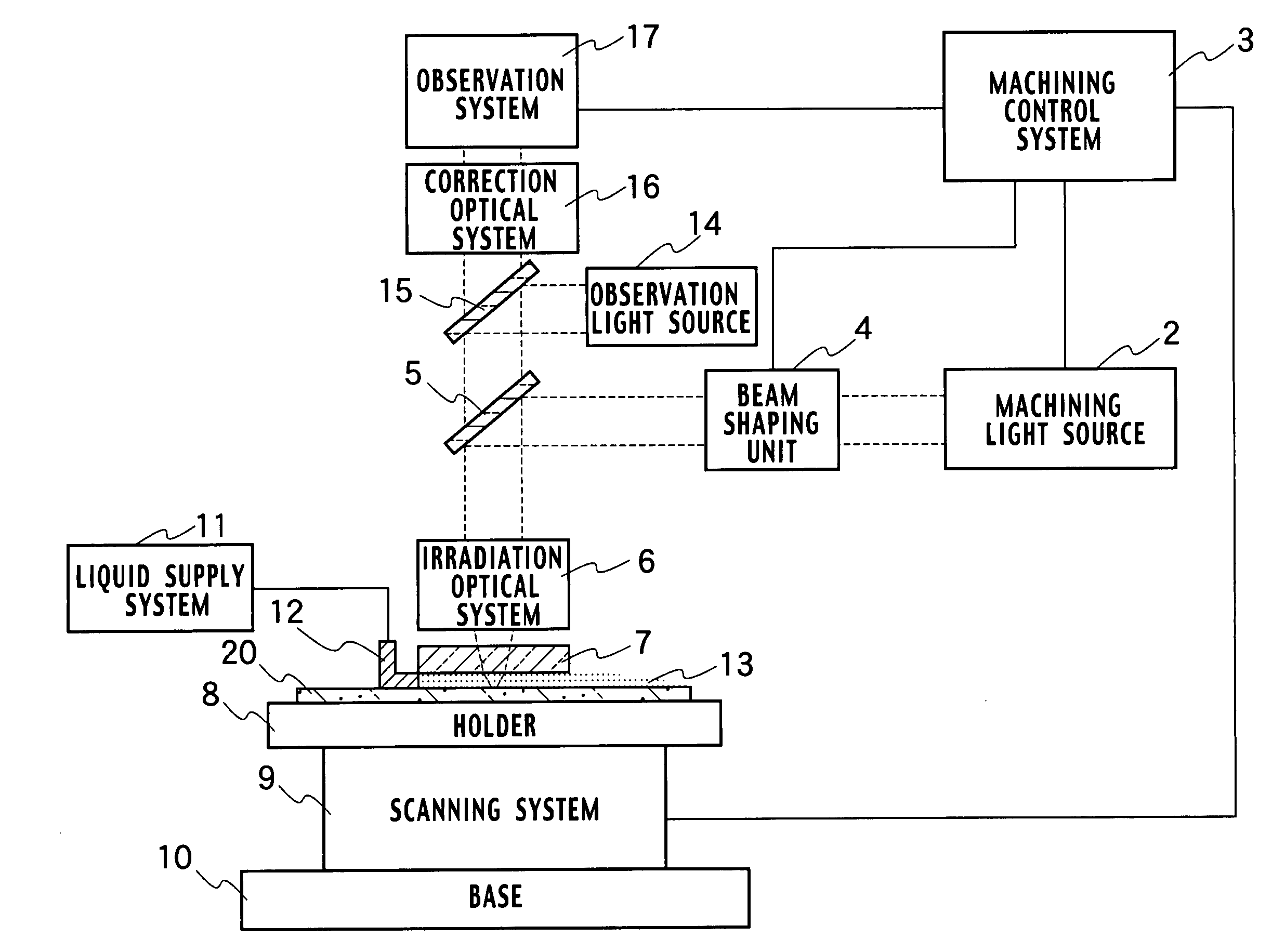
[0051] As shown in FIG. 1, an apparatus for laser beam machining according to a first embodiment of the present invention includes a scanning system 9 configured to move an object 20 to be machining, disposed on a holder 8, in a scanning direction from one end of the object 20 toward the other end thereof. A beam shaping unit 4 includes a machining mask having an asymmetric shaped opening extending in a direction corresponding to the scanning direction of the scanning system 9 on a plane orthogonal to an optical axis direction of a laser beam from a machining light source 2 and includes an optical system so as to output the laser beam which is converted into the asymmetric shape. An irradiation optical system 6 is configured to irradiate the laser beam, which is incident through a half mirror 5 from the beam shaping unit 4, onto the object 20 through a transparent window 7. The scanning system 9 is provided on a base 10.

[0052] In the first embodiment, as th...

second embodiment

[0080] (Second Embodiment)

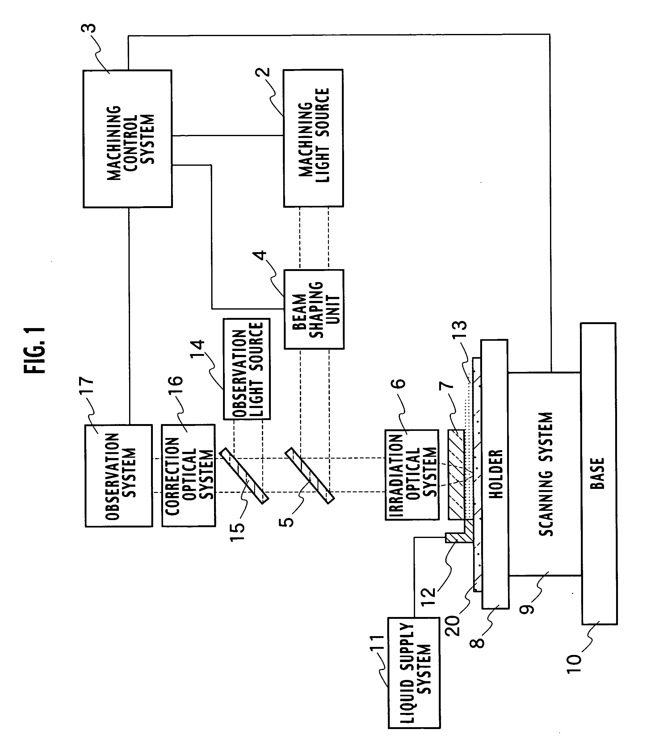
[0081] As shown in FIG. 11, a machining mask 21f according to a second embodiment of the present invention includes openings of a reforming machining opening 29, having slits 27e and 27f facing each other in the opaque portion 22, and a rectangular shaped region machining opening 26f. A longitudinal direction of the slits 27e, 27f corresponds to the scanning direction and the slits 27e, 27f are placed in a front portion of the scanning direction for the region machining opening 26f. In addition, the slits 27e, 27f are placed outside of edges of the region machining opening 26f in the direction orthogonal to the scanning direction and at positions corresponding to portions of the interlevel dielectric films having cracks and stresses, which may be generated by ablation due to the laser beam passing through the region machining opening 26f.

[0082] For example, when the laser beam is irradiated at an irradiation fluence lower than an energy level required for ...

third embodiment

[0093] (Third Embodiment)

[0094] In a third embodiment of the present invention, by use of the laser beam machining apparatus shown in FIG. 1, not only the interlevel dielectric films but also a semiconductor substrate (object) 20 such as Si is processed. In the first and second embodiments, a method for separating semiconductor devices into chips by dicing the semiconductor substrate 20 by use of a blade is applied after removing the interlevel dielectric films in the upper layers by the laser beam machining method. However, if the semiconductor substrate 20 is diced by use of a blade, the semiconductor substrate 20 of a chip is damaged and cracks are generated therein. The damage and cracks of the semiconductor substrate 20 of a chip decrease chip strength of the semiconductor device. Therefore, along with thinning of the chips, machining technology without damage and cracks is desired.

[0095] As the machining method which does not damage the semiconductor substrate 20 and does not...


PUM

PropertyMeasurementUnit
oscillation frequencyaaaaaaaaaa
focal lengthaaaaaaaaaa
optical path lengthaaaaaaaaaa

Abstract

An apparatus for laser beam machining includes a scanning system configured to move an object in a scanning direction from a first edge of the object to another edge of the object; a beam shaping unit configured to convert a laser beam to an asymmetrical machining laser beam in the scanning direction on a plane orthogonal to an optical axis of the laser beam; and an irradiation optical system configured to irradiate the machining laser beam emitted from the beam shaping unit onto the object.

Description

CROSS REFERENCE TO RELATED APPLICATIONS [0001] This application is based upon and claims the benefit of priority from prior Japanese Patent Application P2003-309338 filed on Sep. 1, 2003; the entire contents of which are incorporated by reference herein. BACKGROUND OF THE INVENTION [0002] 1. Field of the Invention [0003] The present invention relates to laser beam machining, more particularly to an apparatus for laser beam machining, which controls dicing by the shape of a laser beam, a machining mask, a semiconductor device, a method for laser beam machining and a method for manufacturing a semiconductor device. [0004] 2. Description of the Related Art [0005] In recent years, in a semiconductor device, a low dielectric constant (low-k) dielectric film has been used to enable operations at higher speed by reducing inter-wiring capacitance. However, when dicing is performed by use of a blade on the semiconductor device having the low-k dielectric film as an interlevel dielectric film...

Claims


Application Information

Patent Timeline
Patent Type & Authority Applications(United States)
IPC IPC(8): B23K26/066B23K26/00B23K26/06B23K26/073B23K26/364B23K101/40H01L21/301H01L21/302H01L21/304H01L21/311H01L21/78
CPCB23K26/0656B23K26/073B23K26/0732B23K26/367H01L33/0095H01L21/3043H01L21/31105H01L21/78B23K2201/40B23K26/066B23K26/364B23K2101/40
Inventor IKEGAMI, HIROSHISEKINE, MAKOTO
Owner KK TOSHIBA
Why Eureka
Try Eureka