Device for ESD protection of an integrated circuit

Inactive Publication Date: 2005-03-03
INFINEON TECH AG
View PDF12 Cites 10 Cited by
  • Summary
  • Abstract
  • Description
  • Claims
  • Application Information

AI Technical Summary

Benefits of technology

[0015] It is a particular object of the invention to provide such a device, which uses components feasible in SOI CMOS technology, so that the device can be fabricated in a standard CMOS process without the need of additional processing steps.
[0016] It is a further particular object of the invention to provide such a device, which is capable of protecting a high frequency integrated circuit against excessive positive and negative voltages.
[0017] It is a yet further object of the invention to provide such a device, which adds a very low parasitic capacitance to the circuit, thereby not essentially affecting the speed of the circuit.
[0018] These objects can be attained, according to the present invention, by a device for electrostatic discharge (ESD) protection of a circuit, particularly a high frequency circuit, of a semiconductor device, wherein the device for ESD protection comprises a first and a second p-type junction field effect transistor (JFET) and a first and second n-type JFET transistor, wherein the first p-type JFET transistor is connected with its gate to a high voltage source, its source to an input/output pad of the semiconductor device, and its drain to the source of the first n-type JFET transistor, the second p-type JFET transistor is connected with its gate to the high voltag

Problems solved by technology

A disadvantage of the prior art solution disclosed in WO03/021737 is that the structure adds to the parasitic capacitance and slows down the circuit.
Further, when using CMOS circuits on thin SOI (Silicon-on-insulator) wafers, where the active silicon layer is at the most a few tenths of micrometer thick, the vertical shunting devices of WO03/021737 a

Method used


Image

  • Device for ESD protection of an integrated circuit
  • Device for ESD protection of an integrated circuit
  • Device for ESD protection of an integrated circuit

Examples


Example

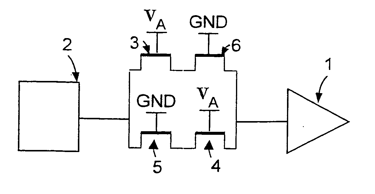
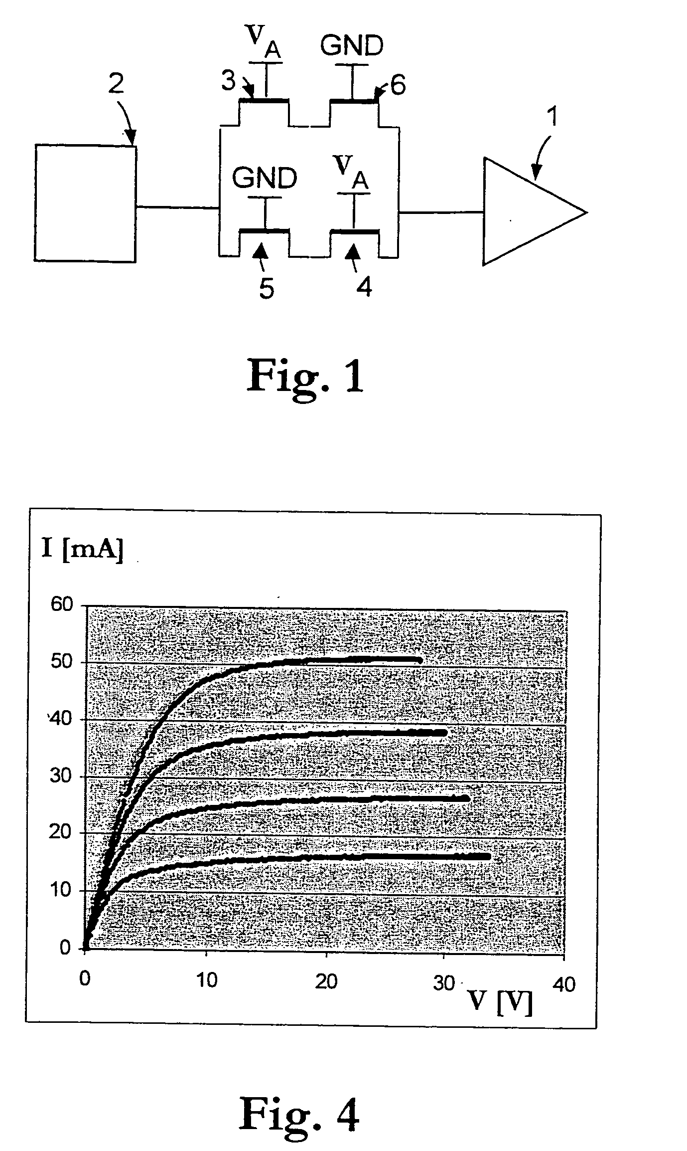
[0028] In FIG. 1 a monolithically integrated ESD protection device according to a preferred embodiment of the present invention is schematically shown. The device includes lateral JFET transistors, which combine the functions of current limitation and current shunting.

[0029] The ESD protection device is interconnected between an input / output terminal of a high frequency or radio frequency MOS circuit 1, e.g. a receiver or driver circuit, and an input / output bonding pad 2. The semiconductor device comprising the MOS circuit 1, the ESD protection device, and the bonding pad 2 is preferably a SOI substrate based device.

[0030] The ESD protection device comprises a first 3 and a second 4 lateral p-type JFET (unction field effect transistor) and a first 6 and second 5 lateral n-type JFET interconnected in a cross-coupled configuration as illustrated.

[0031] That is, the first p-type JFET 3 is connected with its gate to a high voltage source VA of the semiconductor device, its source to ...


PUM


Abstract

A device for ESD protection of a high frequency circuit (1) of a semiconductor device comprises first (3) and second (4) p-type and first (6) and second (5) n-type JFET's, wherein the first p-type JFET (3) is connected with its gate to a high voltage source, its source to an input/output pad (2) of the semiconductor device, and its drain to the source of the first n-type JFET (6), the second p-type JFET (4) is connected with its gate to the high voltage source, its source to the drain of the second n-type JFET (5), and its drain to an input/output terminal of the circuit (1), the first n-type JFET transistor (6) is connected with its gate to ground (GND), and its drain to the input/output terminal, and the second n-type JFET transistor (5) is connected with its gate to ground (GND), and its source to the input/output pad (2).

Description

PRIORITY [0001] This application claims priority to Swedish application No. 0302296-9 filed Aug. 27, 2003. TECHNICAL FIELD OF THE INVENTION [0002] The present invention generally relates to the field of integrated circuit technology, and more specifically the invention relates to a monolithically integrated device for ESD (electrostatic discharge) protection of an integrated circuit. DESCRIPTION OF RELATED ART AND BACKGROUND OF THE INVENTION [0003] Integrated electrostatic discharges may damage electronic devices, particularly electronic semiconductor devices fabricated on insulating or semi-insulating substrates, such as integrated circuits. Devices for protecting against ESD are conventionally incorporated in the input / output paths of most semiconductor devices in order to shunt excessive charge away from the sensitive circuits of the semiconductor devices. [0004] Semiconductor devices are often provided with some protection against high input currents, such as e.g. electrical res...

Claims


Application Information

Patent Timeline
IPC IPC(8): H01LH01L27/02H02H9/00
CPCH01L27/0288H01L27/0266
Inventor LITWIN, ANDREJPETTERSSON, OLA
Owner INFINEON TECH AG
Why Eureka
Try Eureka