This helps you quickly interpret patents by identifying the three key elements:
Problems solved by technology
Method used
Benefits of technology
Benefits of technology
[0012]Further, the oxide semiconductor film is susceptible to damage such as reduction in film thickness by an etchant or change in an amount of oxygen vacancy by plasma. If the damaged semiconductor layer is used for a thin film transistor, characteristics vary. Thus, in the case where an inverted staggered thin film transistor using an oxide semiconductor film is manufactured, a structure in which a channel protective layer protecting a channel formation region from damage is effective. However, in accordance with formation of the channel protective layer, the number of photomasks that are used is increased, a process becomes complicated, and productivity may be decreased.
[0013]It is an object of the present invention to provide a method for manufacturing a thin film transistor in which contact resistance between an oxide semiconductor layer containing indium (In), gallium (Ga), and zinc (Zn) and source and drain electrodelayers is small and in which the oxide semiconductor layer is less damaged in a manufacturing process of the thin film transistor, with a small number of steps.
[0018]Further, since a structure of a thin film transistor to which an embodiment of the present invention is applied is provided with a channel protective layer, not only a channel formation region but also a region opposite to a surface which is in contact with a gate insulating film of an IGZO semiconductor layer, i.e., a back channel can be protected from damage in a process (such as reduction in film thickness by plasma or an etchant in etching or oxidation), whereby reliability of a semiconductor device can be improved.
[0022]According to the present invention, a thin film transistor having a small photocurrent, low parasitic capacitance, a high on-off ratio, and favorable dynamic characteristics (f characteristics) can be manufactured with a small number of steps. Accordingly, a semiconductor device including the thin film transistor having excellent electric characteristics and high reliability can be provided by a method with excellent productivity.
Problems solved by technology
In particular, in the case of manufacturing display devices performing large-area display, the problem of signaldelay due to wiring resistance becomes significant.
In addition, capacitance is caused in a portion where the oxide semiconductor film and the source and drain electrodelayers are directly in contact with each other, and frequency characteristics (referred to as f characteristics) are low, which might hinder rapid operation of the thin film transistor.
Further, the oxide semiconductor film is susceptible to damage such as reduction in film thickness by an etchant or change in an amount of oxygen vacancy by plasma.
However, in accordance with formation of the channel protective layer, the number of photomasks that are used is increased, a process becomes complicated, and productivity may be decreased.
Method used
Image
Click on the blue label to locate the original text in one second.
Reading with bidirectional positioning of images and text.
Examples
embodiment 1
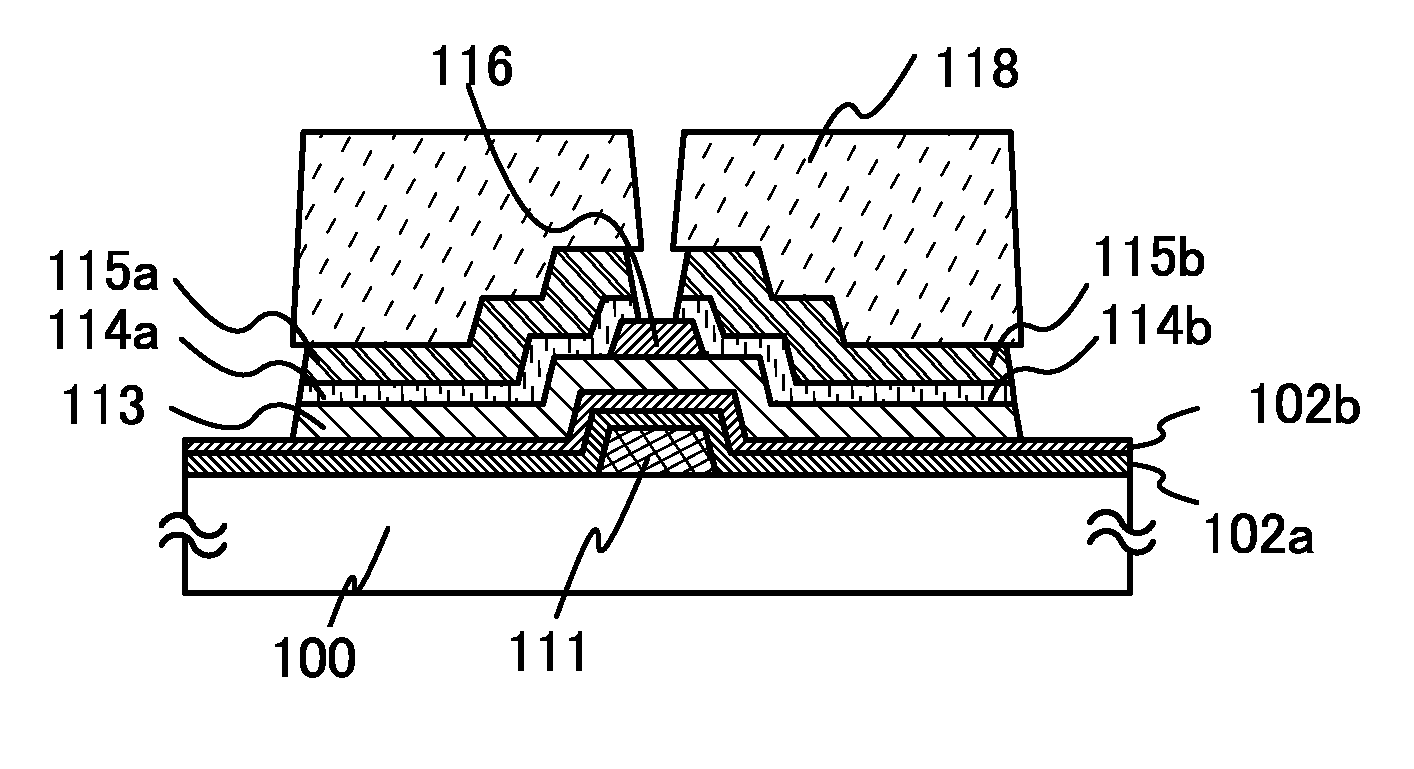
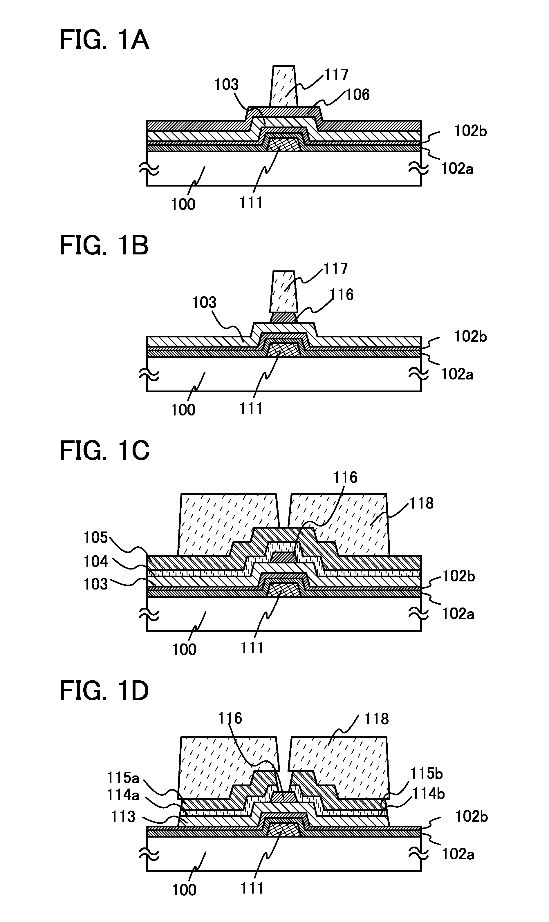
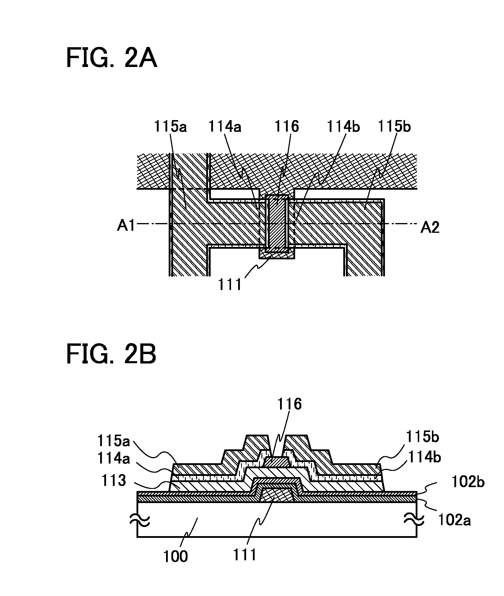
[0049]In this embodiment, a manufacturing process of an inverted staggered (bottom gate) thin film transistor in which an oxide semiconductor layer containing In, Ga, and Zn is used, a buffer layer is provided between the semiconductor layer and source and drain electrode layers, and a channel protective layer is provided is described with reference to FIGS. 1A to 1D and FIGS. 2A and 2B.
[0050]FIGS. 1A to 1D show a manufacturing process of a bottom gate thin film transistor of this embodiment. FIG. 2A is a plane view of a thin film transistor manufactured through steps of FIGS. 1A to 1D, and FIG. 2B is a cross-sectional view taken along a line A1-A2 in FIG. 2A.
[0051]As a substrate 100, any of the following substrates can be used: non-alkaline glass substrates made of bariumborosilicate glass, aluminoborosilicate glass, aluminosilicate glass, and the like by a fusion method or a float method; ceramic substrates; plastic substrates having heat resistance enough to withstand a process ...
embodiment 2
[0111]In this embodiment, a method for manufacturing an inverted staggered (bottom gate) thin film transistor having the structure in which a buffer layer contains an IGZO semiconductor layer, which is different from the structure of Embodiment 1, will be described with reference to FIGS. 3A to 3D and FIGS. 4A and 4B. In addition, in this embodiment, the same reference numerals are used for the same portions as those in Embodiment 1 and detailed description of the portions is omitted.
[0112]FIGS. 3A to 3D illustrate a manufacturing process of a bottom gate thin film transistor of this embodiment. FIG. 4A is a plane view of a thin film transistor manufactured through steps of FIGS. 3A to 3D, and FIG. 4B is a cross-sectional view taken along a line A1-A2 in FIG. 4A.
[0113]In this embodiment, the substrate 100 having a light-transmitting property is used. As the substrate having a light-transmitting property, for example, non-alkaline glass substrates manufactured by a fusion method or a...
embodiment 3
[0128]In this embodiment, a method for manufacturing a thin film transistor in which an IGZO semiconductor layer having a structure in which a plurality of channel formation regions are connected is used is described with reference to FIGS. 5A to 5D.
[0129]FIG. 5A is a cross-sectional view illustrating a state in which the resistmask is formed over the conductive film 105 using a third photomask of this embodiment. FIG. 5B is a cross-sectional view illustrating a state in which the conductive film 105, the film 104 having n-type conductivity, and the semiconductor film 103 are etched. FIG. 5C is a plane view illustrating a completed TFT, and FIG. 5D is a cross-sectional view taken along a line A1-A2 in FIG. 5C. Note that, in this embodiment, the same reference numerals are used for the same portions as those in Embodiment 1 and detailed description of the portions is omitted.
[0130]Gate electrode layers 111a and 111b are formed over the substrate 100 as in Embodiment 1 using a resist...
PUM
Abstract
To provide a method by which a semiconductor device including a thin film transistor with excellent electric characteristics and high reliability is manufactured with a small number of steps. After a channel protective layer is formed over an oxidesemiconductor film containing In, Ga, and Zn, a film having n-type conductivity and a conductive film are formed, and a resistmask is formed over the conductive film. The conductive film, the film having n-type conductivity, and the oxidesemiconductor film containing In, Ga, and Zn are etched using the channel protective layer and gate insulating films as etching stoppers with the resistmask, so that source and drain electrodelayers, a buffer layer, and a semiconductor layer are formed.
Description
BACKGROUND OF THE INVENTION[0001]1. Field of the Invention[0002]The present invention relates to a semiconductor device having a circuit including a thin film transistor (hereinafter referred to as a TFT) using an oxide semiconductor film for a channel formation region and a method for manufacturing the semiconductor device. For example, the present invention relates to an electronic appliance mounted with an electro-optic device typified by a liquid crystal display panel or a light-emitting display device having an organic light-emitting element as a component.[0003]Note that the semiconductor devices in this specification refer to all the devices which can operate by using semiconductor characteristics, and an electro-optic device, a semiconductor circuit, and an electronic appliance are all included in the semiconductor devices.[0004]2. Description of the Related Art[0005]In recent years, active matrix display devices (such as liquid crystal display devices, light-emitting displa...
Claims
Application Information
Patent Timeline
Application Date:The date an application was filed.
Publication Date:The date a patent or application was officially published.
First Publication Date:The earliest publication date of a patent with the same application number.
Issue Date:Publication date of the patent grant document.
PCT Entry Date:The Entry date of PCT National Phase.
Estimated Expiry Date:The statutory expiry date of a patent right according to the Patent Law, and it is the longest term of protection that the patent right can achieve without the termination of the patent right due to other reasons(Term extension factor has been taken into account ).
Invalid Date:Actual expiry date is based on effective date or publication date of legal transaction data of invalid patent.

