Process modules for transport polymerization of low epsilon thin films

a technology of process modules and thin films, applied in the direction of machines/engines, flexible member pumps, positive displacement liquid engines, etc., can solve the problems of unacceptable cross talk and resistance-capacitance delay, rc delay has become a serious problem for ics, and current dielectric materials used in the manufacturing of ics have already proved inadequa

Inactive Publication Date: 2005-03-03
DIELECTRIC SYST INT
View PDF52 Cites 43 Cited by
  • Summary
  • Abstract
  • Description
  • Claims
  • Application Information

AI Technical Summary

Problems solved by technology

During the construction of ICs with shrinking device geometries, an increase in capacitance, mainly on the same layer of interconnects can result in unacceptable cross talk and resistance-capacitance (“RC”) delay.
This RC delay has become a serious problem for ICs with feature size of less than 0.18 μm.
These current dielectric materials used in the manufacturing of the ICs have already proven to be inadequate in several ways for their continued use in mass production of the future IC's.
The present lack of qualified low dielectric materials now threatens to derail the continued shrinkage of future IC's.
However, the decomposition temperature (“Td”) of PPX was too low, and the dielectric constant of the resulting polymer (∈=3.2 to 2.7) was not low enough (Selbrede and Zucker, Proc.
DUMIC Conference, 125-128 (1997) reported that annealing a ...

Method used


Image

  • Process modules for transport polymerization of low epsilon thin films
  • Process modules for transport polymerization of low epsilon thin films
  • Process modules for transport polymerization of low epsilon thin films

Examples


Embodiment Construction

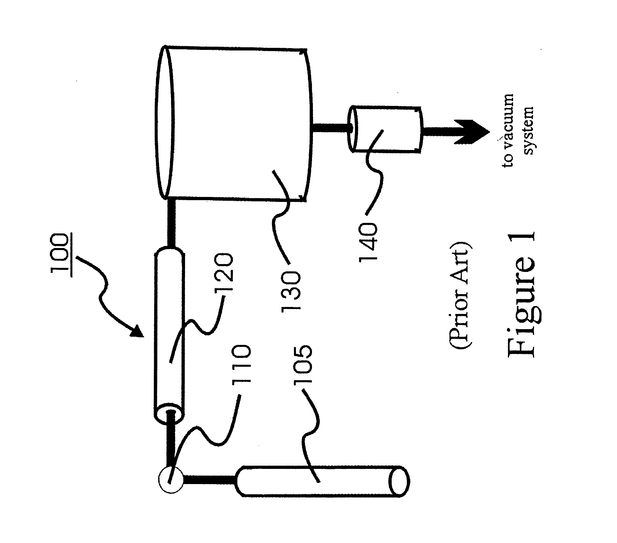
Conventional Chemical Vapor Depostion (“CVD”)

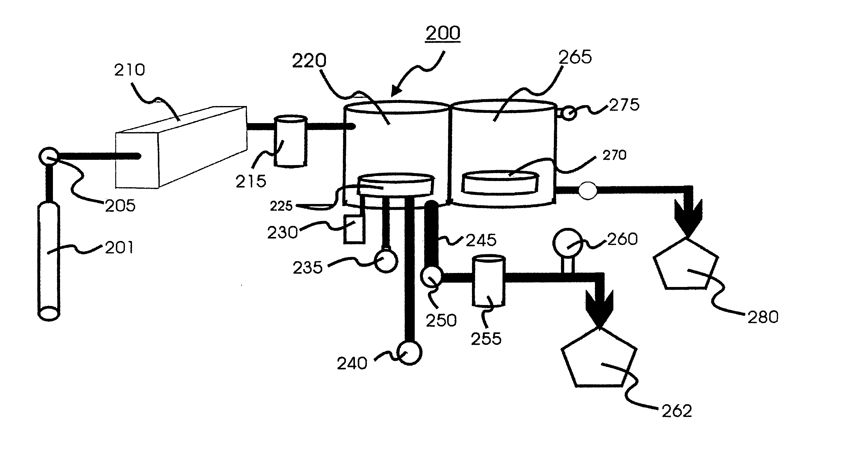
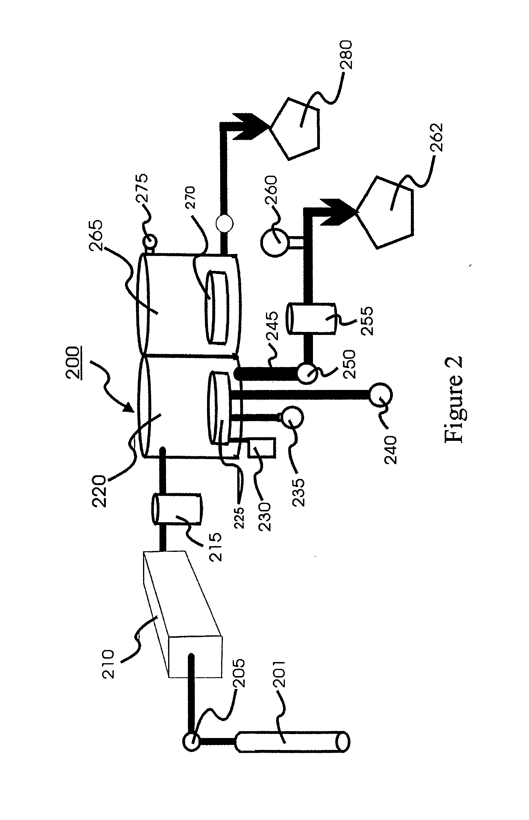
There are several fundamental differences between a transport polymerization (“TP”) process and a conventional Chemical Vapor Deposition (“CVD”) process. Additionally, there are distinctive differences in the Process Module (“PM”) described in the current invention when compared to the PM of a conventional CVD system.

A conventional CVD process begins when the starting chemicals are introduced into a traditional CVD chamber and are subjected to plasma or ozone to generate reacting intermediates. The CVD chamber is normally operated under sub-atmosphere pressure, or even moderate vacuum in the ranges of few mTorrs to few Torrs. A wafer is heated at high temperatures to remove any unstable products. A film grows not only the wafer surface but also on other surfaces inside a deposition chamber. Such non-selective deposition requires frequently cleaning for these surfaces inside the CVD chamber. Traditional CVD process that utilizes. ozon...


PUM

PropertyMeasurementUnit
Temperatureaaaaaaaaaa

Abstract

A Process Module (“PM”) is designed to facilitate Transport Polymerization (“TP”) of precursors that are useful for preparations of low Dielectric Constant (“∈”) films. The PM consists primarily of a Material Delivery System (“MDS”) with a high temperature Vapor Phase Controller (“VFC”), a TP Reactor, a Treatment Chamber, a Deposition Chamber and a Pumping System. The PM is designed to facilitate TP for new precursors and for film deposition and stabilization processes.

Description

BACKGROUND This invention is related to a polymer deposition system that is useful for the fabrication of an integrated circuit (“IC”). In particular, this invention is related to Process Module (“PM”) used for deposition of low dielectric (“∈”) thin films. Furthermore, this invention discloses chemistries of precursor and methods for utilization of the PM to convert the precursor into dielectric thin film. During the construction of ICs with shrinking device geometries, an increase in capacitance, mainly on the same layer of interconnects can result in unacceptable cross talk and resistance-capacitance (“RC”) delay. This RC delay has become a serious problem for ICs with feature size of less than 0.18 μm. Thus, the dielectric constant of the current insulation materials from which IC's are constructed must be decreased to meet the needs for fabrication of future ICs. In addition to dielectric and conducting layers, the “barrier layer” may include metals such as Ti, Ta, W, and Co ...

Claims


Application Information

Patent Timeline
IPC IPC(8): B05D1/00B05D3/06B05D7/24C23C16/452H01L21/312
CPCB05D1/007B05D1/60B05D3/062C23C16/452H01L21/02348H01L21/3127H01L21/02118H01L21/02271H01L21/312H01L21/02205
Inventor LEE, CHUNG J.NGUYEN, OANHLEE, WEI SHIANG CHARLESSOLOMENSKY, MICHAELKUMAR, ATULCHUNG CHANG, JAMES YUNGUYEN, BINH
Owner DIELECTRIC SYST INT
Why Eureka
Try Eureka