Luminescent efficiency of semiconductor nanocrystals by surface treatment
- Summary
- Abstract
- Description
- Claims
- Application Information
AI Technical Summary
Benefits of technology
Problems solved by technology
Method used
Image

Examples
example 1
Synthesis of CdS Nanocrystal's and Surface Treatment
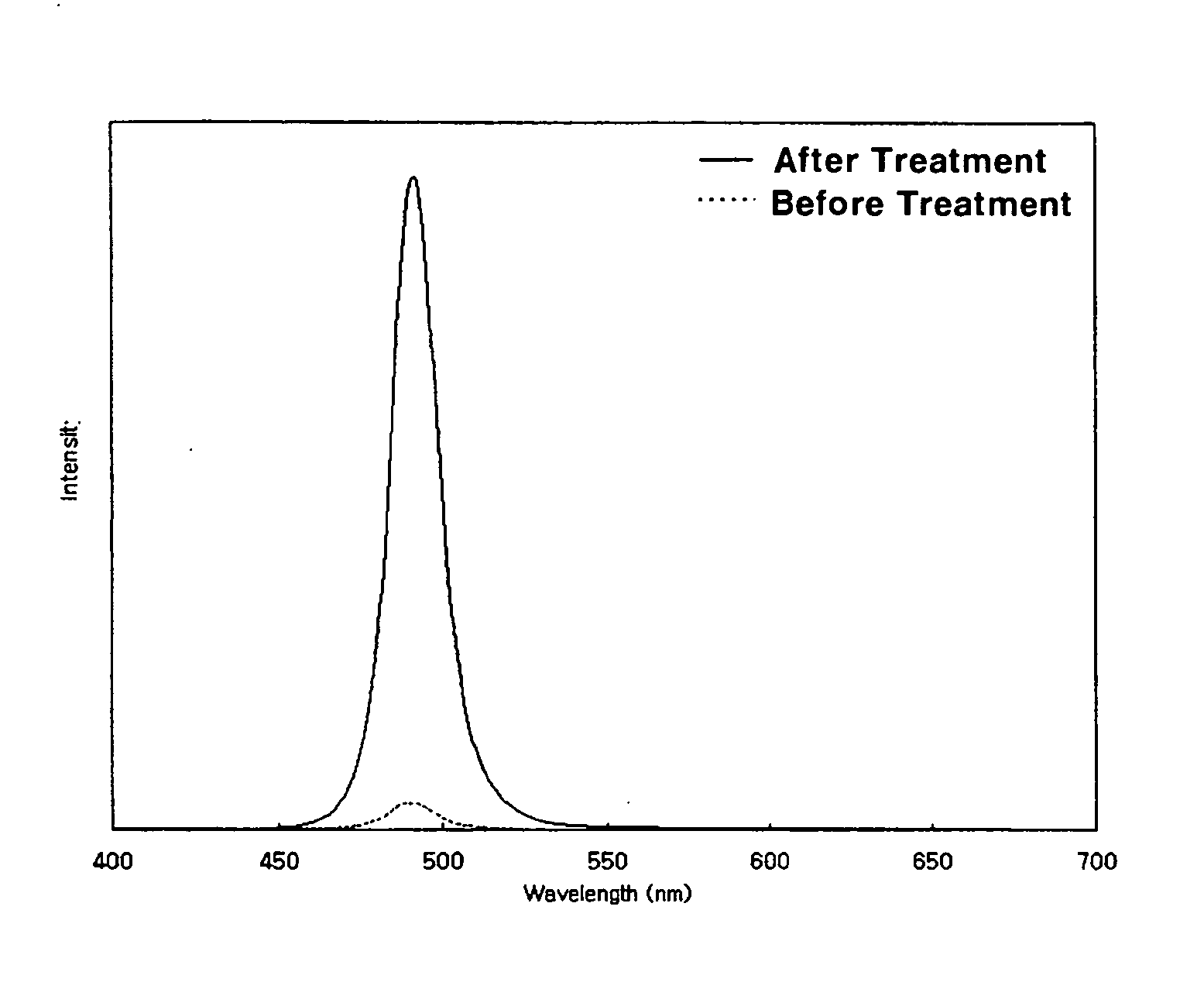
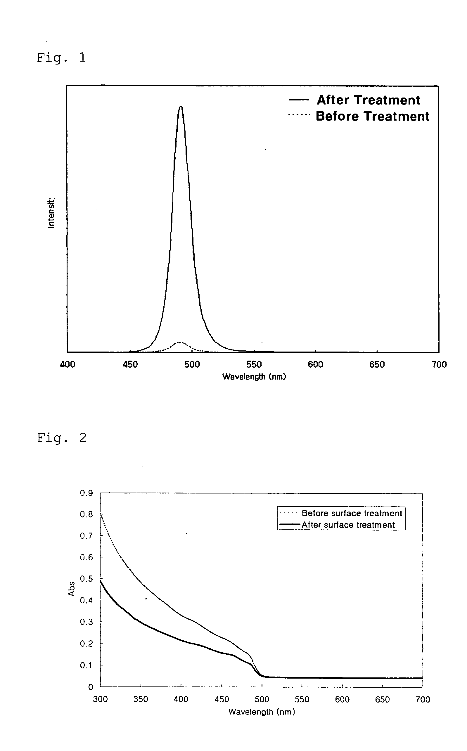
[0048] 16 g of trioctyl amine (hereinafter, referred to as ‘TOA’, 1.9 g of oleic acid and 1.6 mmol of cadmium oxide are charged simultaneously into a 125 ml flask equipped with a reflux condenser. The mixture is heated to 300° C. with stirring. Separately, a sulfur (S) powder is dissolved in trioctyl phpsphine (hereinafter, referred to as ‘TOP’) to form an S-TOP complex solution in a sulfur concentration of about 0.1M. 1.0 ml of the S-TOP solution is rapidly fed to the previous mixture, and then reacted for 2 minutes with stirring. Immediately after the reaction is completed, the reaction mixture is cooled to room temperature. Ethanol as a non-solvent is added to the reaction mixture, and the resulting mixture is then centrifuged. The precipitates are separated by decanting the solution and dispersed in 8 ml of toluene to obtain a solution of CdS nanocrystals in toluene. 1 ml of the CdS solution is sampled and about 0.02 g of NaBH...
example 2
Synthesis of CdTe Nanocrystals and Surface Treatment
[0050] 16 g of TOA, 0.5 g of oleic acid and 0.2 mmol of cadmium acetate are charged simultaneously into a 125 ml flask equipped with a reflux condenser. The mixture is heated to 180° C. with stirring. Separately, a Te powder is dissolved in TOP to form a Te-TOP complex solution in a Te concentration of about 0.2M. 0.5 ml of the Te-TOP solution is rapidly fed to the previous mixture, and then reacted for 30 seconds with stirring. Immediately after the reaction is completed, the reaction mixture is cooled to room temperature. Ethanol as a non-solvent is added to the reaction mixture, and the resulting mixture is then centrifuged. The precipitates are separated by decanting the solution and dispersing them in 5 ml of toluene to obtain a solution of CdTe nanocrystals in toluene. 1 ml of the CdTe solution is sampled and about 0.02 g of NaBH4 is added thereto. The resulting mixture is stirred at room temperature for about 10 minutes to ...
example 3
Synthesis of CdSeS Nanocrystals and Surface Treatment
[0051] 16 g of TOA, 0.5 g of oleic acid and 0.4 mmol of cadmium oxide are charged simultaneously into a 125 ml flask equipped with a reflux condenser. The mixture is heated to 300° C. with stirring. Separately, a Se powder is dissolved in TOP to form a Se-TOP complex solution in a Se concentration of about 0.25M, and a S powder is then dissolved in TOP to form an S-TOP complex solution in a S concentration of about 1.0M. 0.9 ml of the S-TOP solution and 0.1 ml of the Se-TOP solution are rapidly fed to the previous mixture, and then reacted for 4 minutes with stirring. Immediately after the reaction is completed, the reaction mixture is cooled to room temperature. Ethanol as a non-solvent is added to the reaction mixture, and the resulting mixture is then centrifuged. The precipitates are separated by decanting the solution and dispersed in 10 ml of toluene to obtain a solution of CdSeS nanocrystals in toluene. 1 ml of the CdSeS s...
PUM
 Abstract
Description
Claims
Application Information
 - Generate Ideas
- Intellectual Property
- Life Sciences
- Materials
- Tech Scout
- Unparalleled Data Quality
- Higher Quality Content
- 60% Fewer Hallucinations
Browse by: Latest US Patents, China's latest patents, Technical Efficacy Thesaurus, Application Domain, Technology Topic, Popular Technical Reports.
© 2025 PatSnap. All rights reserved.Legal|Privacy policy|Modern Slavery Act Transparency Statement|Sitemap|About US| Contact US: help@patsnap.com