Semiconductor device and method of manufacturing thereof
Inactive Publication Date: 2005-03-17
SEMICON ENERGY LAB CO LTD
View PDF69 Cites 85 Cited by
Summary
Abstract
Description
Claims
Application Information
AI Technical Summary
This helps you quickly interpret patents by identifying the three key elements:
Problems solved by technology
Method used
Benefits of technology
Benefits of technology
[0038] According to the present invention, a semiconductor device including a semiconductor element having a polysilicon film as an active region and a semiconductor element having an amorphous silicon film as an active region can be formed over a plastic substrate. Namely, an optical sensor, a photoelectric conversion element, a solar battery element, or the like including a TFT having an active region made of a polysilicon film and a diode having an active region made of an amorphous silicon film can be manufactured.
[0039] A semiconductor device manufactured according to the present invention can be made more lightweight and thinner compared with a conventional one, since it is formed over a plastic substrate.
[0040] In the case where a semiconductor device is an optical sensor or a photoelectric conversion device, a signal detected by a photoelectric conversion element can be amplified by an amplifying element formed of a TFT having a polysilicon film as an active region. Therefore, weak visible light can be detected even when light receiving area of the sensor is small.
[0041] Further, it can be made thinner since a plastic substrate is used. Then, selectivity of an installation site is improved; accordingly, area of a mounting substrate can be reduced. In addition, light receiving area of an optical sensor, a photoelectric conversion element, or a solar battery element can be enlarged.
Problems solved by technology
Consequently, in the case of sensing a white fluorescent light which hardly includes a spectrum of an infrared region and sunlight which has a wide range of spectra from an ultraviolet region to an infrared region, there is a problem that detected results of each light are different even though actual illuminance is equal.
Therefore, response speed thereof is slow, and a dynamic range due to contrast of light is narrow.
However, a capacitor for retaining a charge or an element for amplifying and outputting an optical charge is required since current due to the optical charge is small.
However, cost is very high since as many bare chip ICs as the optical sensors are required.
Therefore, occupied area in an installation substrate such as a printed wiring board is enlarged, which becomes an obstacle to downsizing of an electronic device equipped with the optical sensor.
Further, a cost thereof is low compared with that of the IC type optical sensor using single crystalsilicon.
H6-275808, has limitation on the kind of a substrate due to its manufacturing process.
These substrates have thick film thickness, which causes a problem of increase in parts volume and weight of the optical sensor.
Since glass or the like does not have flexibility, an installation site of the optical sensor is over a flat portion, specifically, over a printed wiring board, and there is limitation on the installation site.
Plastic is lightweight and thin; however, it has a low allowable temperature limit.
There is a problem that it is difficult to form the TFT having an active region made of a polysilicon film over this substrate.
Method used
Image
Click on the blue label to locate the original text in one second.
Reading with bidirectional positioning of images and text.
Examples
embodiment mode 1
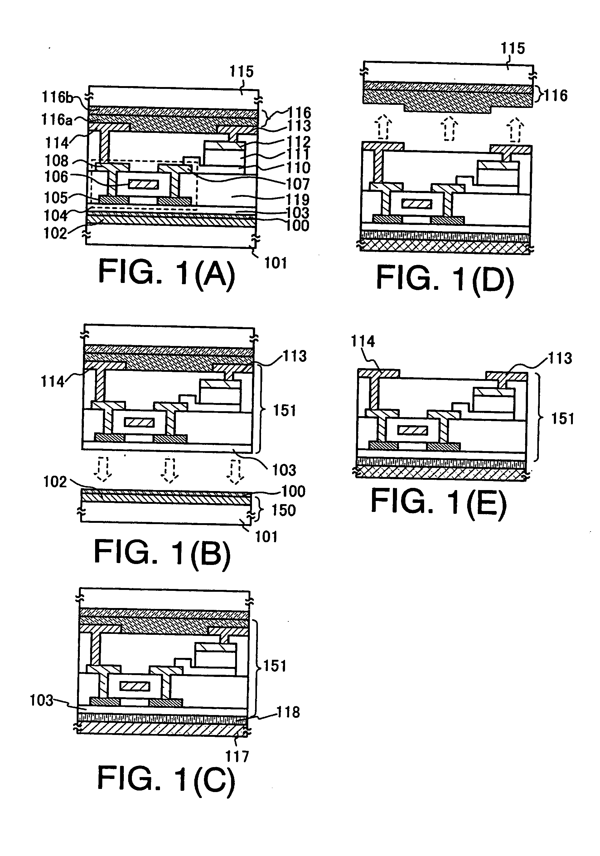
[0054] A method for manufacturing a semiconductor device including a semiconductor element having an amorphous silicon film as an active region and a semiconductor element having a polysilicon film as an active region over a plastic substrate is described in this embodiment mode with reference to FIGS. 1(A) TO 1(E).
[0055] First, a metal film 102 is formed over a substrate 101. A single layer made of one element of W, Ti, Ta, Mo, Cr, Nd, Fe, Ni, Co, Zr, Zn, Ru, Rh, Pd, Os, and Ir or an alloy material or a compound material containing the element as its main component, a laminate thereof, a single layer of nitride thereof, or a laminate thereof may be used as the metal film 102. A film thickness of the metal film 102 is set from 10 nm to 200 nm, preferably, from 50 nm to 75 nm.
[0056] Next, an insulating film 103 is formed over the metal film 102. At this time, a metal oxide film 100 in an amorphous state is formed between the metal film 102 and the insulating film 103 to have a thic...
embodiment mode 2
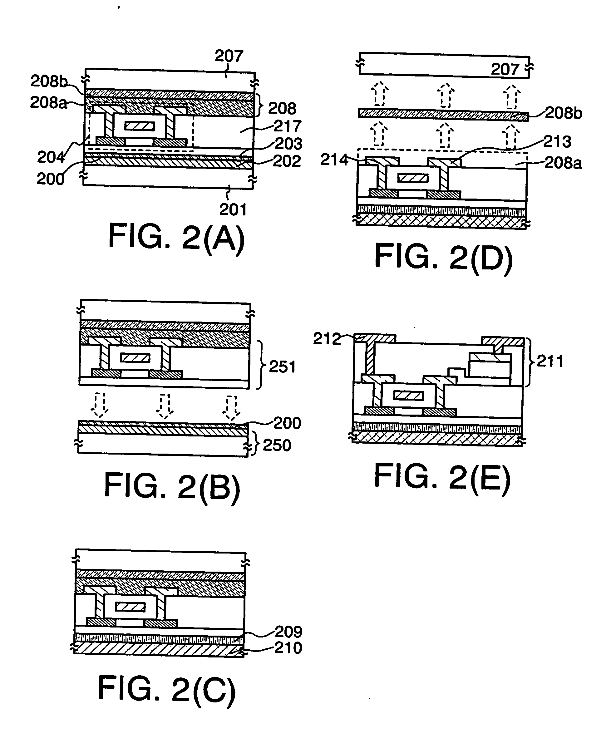
[0083] A method for manufacturing a semiconductor device over a plastic substrate, typically, a flexible plastic substrate in a different way from that in Embodiment Mode 1 is described in this embodiment mode with reference to FIGS. 2(A) to 2(E).
[0084] As in Embodiment Mode 1, a metal film 202, an insulating film 203, and a TFT 204 are sequentially formed over a first substrate 201 as shown in FIG. 2(A). At this time, a metal oxide film 200 in an amorphous state is formed between the metal film 202 and the insulating film 203 to have a thickness of approximately from 2 nm to 5 nm, as in Embodiment Mode 1.
[0085] Note that the TFT 204 includes a polysilicon film having a source region, a drain region, and a channel formation region, a gate insulating film covering the polysilicon film, a gate electrode formed over the channel formation region of the polysilicon film, and a source electrode and a drain electrode which are connected to the source region and the drain region through a...
embodiment
EMBODIMENT 1
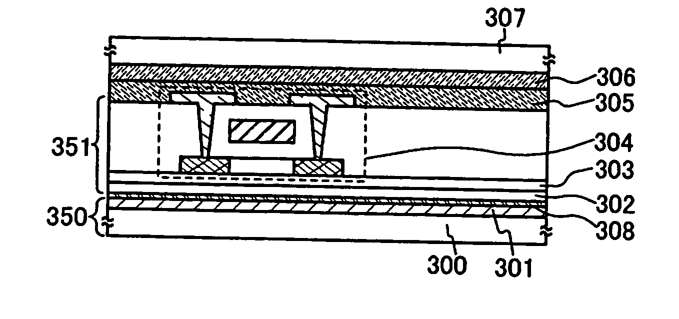
[0096] An example of manufacturing an optical sensor including a TFT having a polysilicon film as an active region and a diode having an amorphous silicon film as an active region by using the steps of Embodiment Mode 2 is described in this embodiment with reference to FIGS. 3(A) to 3(D). Note that the optical sensor of this embodiment is a non-storage type optical sensor.
[0097] A TFT 304 is formed over a glass substrate (first substrate 300) as shown in FIG. 3(A). A metal film 301, here, a tungsten film (film thickness: 80 nm) is formed over the glass substrate by a sputtering method, and further, an insulating film 302, here, a siliconoxide film (film thickness: 160 nm) is laminated without being exposed to atmospheric air by a sputtering method. At this time, a tungsten oxide film 308 in an amorphous state is formed between the tungsten film 301 and the silicon oxide film 301 to have a thickness of approximately from 2 nm to 5 nm. Since the tungsten film and the si...
PUM
Abstract
The manufacturing method of a semiconductor device according to the present invention comprises steps of forming a metal film, an insulating film, and an amorphous semiconductor film in sequence over a first substrate; crystallizing the metal film and the amorphous semiconductor film; forming a first semiconductor element by using the crystallized semiconductor film as an active region; attaching a support to the first semiconductor element by using an adhesive; causing separation between the metal film and the insulating film; attaching a second substrate to the separated insulating film; separating the support by removing the adhesive; forming an amorphous semiconductor film over the first semiconductor element; and forming a second semiconductor element using the amorphous semiconductor film as an active region.
Description
BACKGROUND OF THE INVENTION [0001] 1. Field of the Invention [0002] The present invention relates to a method of manufacturing a thin and lightweight semiconductor device. Specifically, the present invention relates to a method for manufacturing a semiconductor device over an organic resin member or a plastic substrate. In the present invention, a semiconductor device is a semiconductor device including a semiconductor element having an amorphous semiconductor film as an active region and a semiconductor element having a crystalline semiconductor film as an active region, specifically, a semiconductor device including an optical sensor element, a photoelectric conversion device, a solar battery, or the like. [0003] 2. Description of Related Art [0004] An optical sensor is used as a sensor for converting an image into an electrical signal in a wide range of fields such as a facsimilemachine, a copyingmachine, a video camera, and a digital still camera. Mainly, a semiconductor is us...
Claims
Application Information
Patent Timeline
Application Date:The date an application was filed.
Publication Date:The date a patent or application was officially published.
First Publication Date:The earliest publication date of a patent with the same application number.
Issue Date:Publication date of the patent grant document.
PCT Entry Date:The Entry date of PCT National Phase.
Estimated Expiry Date:The statutory expiry date of a patent right according to the Patent Law, and it is the longest term of protection that the patent right can achieve without the termination of the patent right due to other reasons(Term extension factor has been taken into account ).
Invalid Date:Actual expiry date is based on effective date or publication date of legal transaction data of invalid patent.

