Gallium nitride compound semiconductor device and method of manufacturing the same

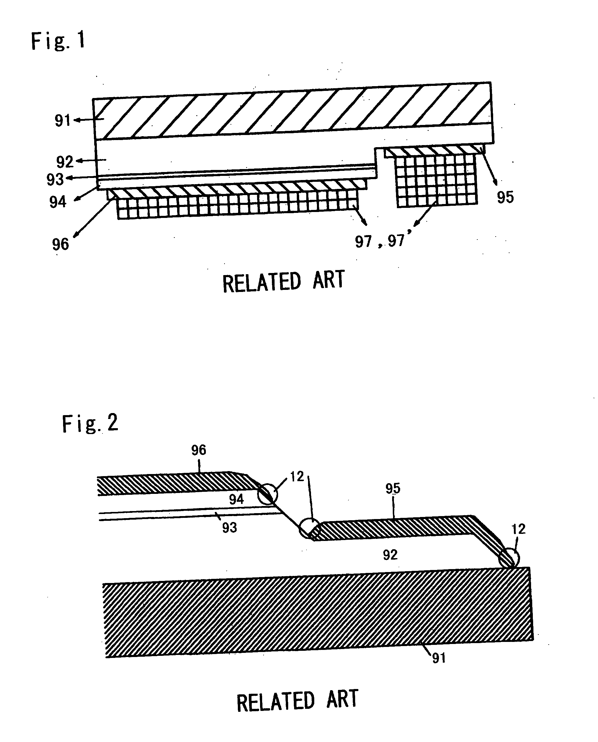
a gallium nitride and compound semiconductor technology, applied in the direction of printing, printing, other printing apparatus, etc., can solve the problems of imperfect cleaning, surface contamination and oxidation, poor electric characteristics of p-type gan electrodes formed thereon, etc., to prevent deterioration in ohmic characteristics and reflectivity, reduce the total time needed, and reduce the number of times of evaporation

Active Publication Date: 2005-03-17
STANLEY ELECTRIC CO LTD
View PDF1 Cites 16 Cited by
  • Summary
  • Abstract
  • Description
  • Claims
  • Application Information

AI Technical Summary

Benefits of technology

[0048] One of several benefits of the present invention is that it can eliminate the need for annealing in forming the electrodes of the GaN type device. While annealing may still be done to the GaN type devices, it is not necessary. Thus, if little or no annealing is done, a wafer will not accumulate a needless heat history, and the electrodes being processed can be prevented from deteriorating in ohmic characteristics and reflectivity. After the formation of the electrode for n-type or p-type GaN, the eutectic electrode having an Au / Sn laminate structure or the like can be laminated thereon successively without the in-process article being taken out of the vacuum evaporation system. This allows a significant reduction of the total time necessary for the device manufacturing process. Moreover, since the in-process article is not necessarily taken out of the vacuum evaporation system, it is possible to avoid contamination and surface oxidation of the electrode for p-type or n-type GaN. The number of times of evaporation can also be reduced. Another advantage is that the process design has a higher degree of freedom since heat-sensitive organic materials can also be used.
[0049] Annealing, when conducted, produces stress due to a difference between the coefficients of thermal expansion of the GaN layer and the electrode material. Accordingly, it is desirable to have a smaller heat history on the electrode material to make the stress accumulation significantly smaller. This can suppress electrode exfoliation for improved reliability.

Problems solved by technology

In any of the above cases, establishing ohmic contact with a gallium nitride compound semiconductor requires annealing at or above 400° C. This causes several problems as follows: (1) A first problem is evident in that surface contamination and oxidation are inevitable in the annealing furnace.
This inevitably contaminates the surface with impurities in the furnace and causes surface oxidation, so that the p-type GaN electrodes formed thereon become poor in electric characteristic.
Even if the electrode-forming surface is cleaned to alleviate contamination and surface oxidation, the n-type GaN electrodes that are formed already preclude cleaning processes that can affect the material of the electrodes.
This results in imperfect cleaning.
In addition, the presence of the annealing even after the formation of the p-type GaN electrodes can give the n-type GaN electrodes an excessive heat history.
The two annealing processes thus result in poorer electric characteristics.
The same problems can also occur when the p-type GaN electrodes are formed first.
Consequently, the other electrodes which would exhibit optimum ohmic characteristics at milder conditions are inevitably deteriorated in characteristic.
Such a material, however, has not been adequately found so far.
This applies excessive heat to the n-type GaN electrode 95 resulting in deterioration in electric characteristics.
(2) A Second Problem Lies in that the Device Process is Limited.
In general, when annealed at excessive temperatures, each of the n-type GaN electrodes and p-type GaN electrodes is coarsened at the surface of its metal layer on the semiconductor-layer side, with an unfavorable deterioration in reflectivity and ohmic characteristic.
In addition, the annealing temperature cannot be optimized.
This inevitably causes the problems that the device process cannot be designed freely, and device characteristics cannot be optimized.

Method used


Image

  • Gallium nitride compound semiconductor device and method of manufacturing the same
  • Gallium nitride compound semiconductor device and method of manufacturing the same
  • Gallium nitride compound semiconductor device and method of manufacturing the same

Examples


Embodiment Construction

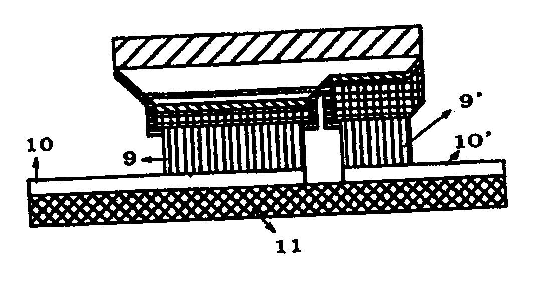
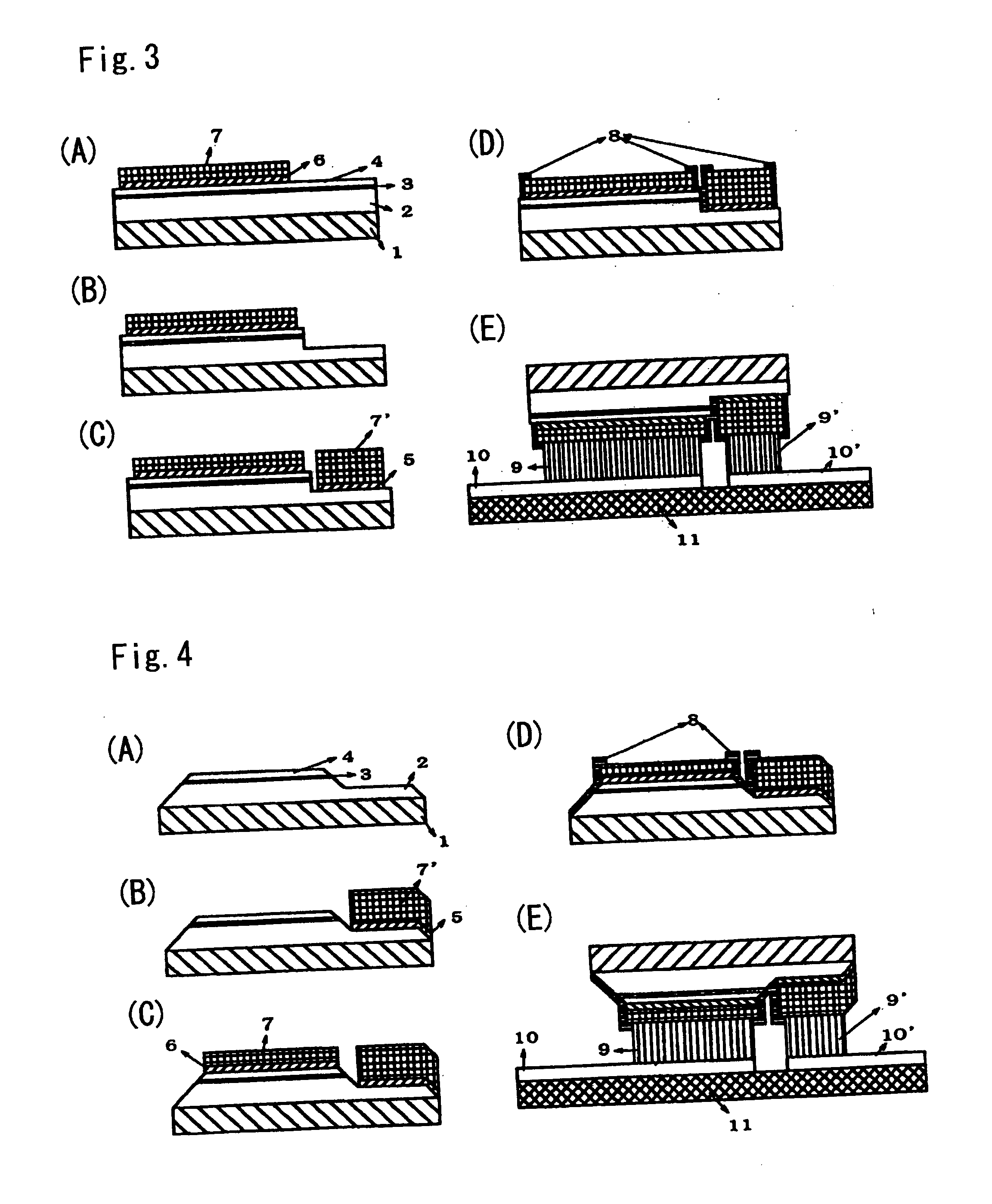
[0060] Hereinafter, detailed description will be given of embodiments of the present invention. The described embodiments of FIGS. 3 and 4 are predicated on a mounting method of flip chip type. It is understood, however, that the present invention is also applicable in the cases of face-up type in which the light output surface is on the semiconductor side. The described embodiments are just a few examples of experiments which the inventors have made for the sake of confirming the effect of the present invention. The present invention must not be considered as limited to the embodiments described herein.

[0061] A device wafer having a silicon (Si) doped n-type GaN layer 2, an active layer 3 made of a gallium nitride aluminum indium compound, and a magnesium (Mg) doped p-type GaN layer 4 via a buffer layer on a sapphire substrate 1 was formed by MOCVD. Then, this wafer was subjected to the following process, which will be described with reference to FIG. 3.

[0062] (1) The wafer was s...


PUM

PropertyMeasurementUnit
thicknessaaaaaaaaaa
thicknessaaaaaaaaaa
thicknessaaaaaaaaaa

Abstract

A GaN compound semiconductor device can be capable of free process design and can have optimum device characteristics. The device can include a group III nitride compound semiconductor laminate structure including an n-type GaN compound semiconductor layer and a p-type GaN compound semiconductor layer. An n electrode can be formed on the n-type GaN compound semiconductor layer, and a p electrode can be formed on the p-type GaN compound semiconductor layer. The n electrode preferably includes an Al layer of 1 to 10 nm, in contact with the n-type GaN compound semiconductor layer, and any metal layer of Rh, Ir, Pt, and Pd formed on the Al layer. The p electrode can be made of a 200 nm or less layer of of Pd, Pt, Rh, Pt/Rh, Pt/Ag, Rh/Ag, Pd/Rh, or Pd/Ag, in contact with the p-type GaN compound semiconductor layer. Both electrodes can make ohmic contact with respective n-type/p-type GaN semiconductors without application of active annealing.

Description

[0001] This application claims the priority benefit under 35 U.S.C. §119 of Japanese Patent Application No. 2003-322437, filed on Sep. 16, 2003, and Japanese Patent Application No. 2004-210876, filed on Jul. 20, 2004, which are hereby incorporated by reference. BACKGROUND OF THE INVENTION [0002] 1. Filed of the Invention [0003] The present invention relates to a device made of gallium nitride compound semiconductors. In particular, the invention relates to a device having electrodes best suited to gallium nitride compound semiconductors, and a method (device process) of manufacturing the device. [0004] 2. Description of the Related Art [0005]FIG. 1 shows a conventional gallium nitride compound semiconductor light-emitting device. This light-emitting device is shown with its electrode side downward since it is mounted on feeding electrodes (not-shown) in a flip chip fashion. This light-emitting device has an n-type gallium nitride compound semiconductor layer 92 (hereinafter, referre...

Claims


Application Information

Patent Timeline
Patent Type & Authority Applications(United States)
IPC IPC(8): H01L21/28H01L21/285H01L33/10H01L33/32H01L33/40H01L33/62
CPCH01L21/28575H01L33/40H01L33/0095H01L33/007H01L2224/14
Inventor TSUCHIYA, MASAHIKOHORIO, NAOCHIKAMORIKAWA, KENICHI
Owner STANLEY ELECTRIC CO LTD
Why Eureka
Try Eureka