CMOS image sensor and method for manufacturing the same

a technology of image sensor and manufacturing method, which is applied in the direction of diodes, semiconductor devices, radio frequency controlled devices, etc., can solve the problems of high power consumption, complicated manufacturing process, and complicated drive mode, and achieve the effect of reducing the dark current of the cmos image sensor

Inactive Publication Date: 2005-03-24
DONGBUANAM SEMICON
View PDF4 Cites 26 Cited by
  • Summary
  • Abstract
  • Description
  • Claims
  • Application Information

AI Technical Summary

Benefits of technology

[0034] In another aspect, a Po type diffusion region is formed on the n− type diffusion region of the photo diode so as to reduce dark current generated on the surface of the semiconductor substrate.
[0035] In accordance with the present invention, the passivation layer composed of insulating layer is formed as a masking layer to prevent a

Problems solved by technology

A CCD has various disadvantages, such as complicated drive mode, high power consumption, complicated manufacturing process, i.e., a large number of processing steps, and so forth.
Additionally, a CCD has a disadvantage in that it is difficult to make a compact-size product, due to the difficulty in integrating various circuits such as a controlling circuit, a signal processing circuit, analog/digital converting circuit and so on into a single chip.
The conventional CMOS image sensor 100 with such a structure has disadvantages such as degradations of the performance and electric charge storing capacity, due to an increase of dark current, which is generated by electrons being transferred to the floating diffusion region from the photo diode 110 when no light is received by the photo diode 110.
The defects may cause a generation of electron or hole c

Method used


Image

  • CMOS image sensor and method for manufacturing the same
  • CMOS image sensor and method for manufacturing the same
  • CMOS image sensor and method for manufacturing the same

Examples


Embodiment Construction

[0044] Hereinafter, an embodiment of the present invention will be described with reference to the accompanying drawings. In the following description and drawings, the same reference numerals are used to indicate the same or similar components. A P++ type means a high concentration P type, a Po type means a medium concentration P type, and an n− type means a low concentration n type.

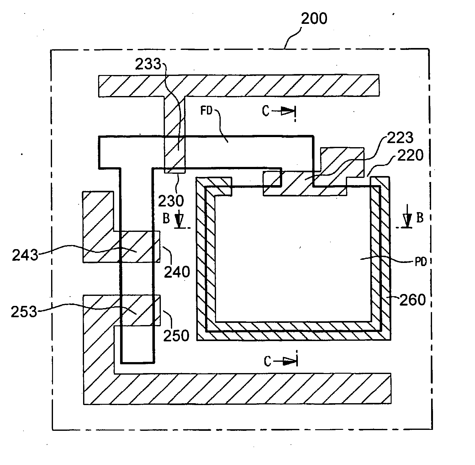
[0045]FIG. 4 is a layout of a unit pixel 200 of a CMOS image sensor according to an embodiment of the present invention.

[0046] Referring to FIG. 4, in unit pixel 200, a solid line indicates an active region wherein a photo diode PD is to be formed, and is defined by an isolation region (not shown) formed surrounding the active region. The gates 223, 233, 243 and 253, respectively of a transfer transistor 220, a reset transistor 230, a drive transistor 240 and a select transistor 250 are disposed as shown in FIG. 4.

[0047] Furthermore, in order to prevent the boundary portion of the active region from ...


PUM


Abstract

A CMOS image sensor and a manufacturing method thereof, wherein the gates of several transistors of the CMOS image sensor are formed in an active region defined by an isolation region for a unit pixel of the CMOS image sensor, and a passivation layer composed of insulating layer is formed on the semiconductor substrate. Impurities are ion-implanted into the active region to form one or more diffusion regions of a photo diode of the CMOS image sensor, wherein the passivation layer prevents a boundary portion of the active region from being ion-implanted. Thus, damages by ion implantation at the boundary portion between the diffusion region for the photo diode and the isolation region are prevented, and the dark current of the CMOS image sensor is reduced.

Description

[0001] This application is based on and claims priority to Korean Patent Application No. 10-2003-0065730, filed Sep. 23, 2003, the entire contents of which are incorporated herein by reference. BACKGROUND OF THE INVENTION [0002] 1. Field of the Invention [0003] The present invention relates to a CMOS image sensor, and more particularly to a CMOS image sensor and method for manufacturing the same, in which a diffusion region of a photo diode is disposed apart from an isolation region, and thereby a dark current is reduced. [0004] 2. Description of the Prior Art [0005] In general, an image sensor is a semiconductor device for converting an optical image into electrical signals, and is generally classified into a charge coupled device (CCD) and a complementary MOS (CMOS) image sensor. [0006] A CCD generally includes a plurality of MOS capacitors and each MOS capacitor is adjacently disposed to each other. Charge carriers are stored on one of the MOS capacitors and then transferred to a...

Claims


Application Information

Patent Timeline
IPC IPC(8): H01L27/146H01L31/062
CPCH01L27/14687H01L27/14643H01L27/146
Inventor HAN, CHANG HUN
Owner DONGBUANAM SEMICON
Why Eureka
Try Eureka