Memory cell unit, nonvolatile semiconductor storage device including memory cell unit, and memory cell array driving method

a memory cell and nonvolatile technology, applied in the direction of digital storage, instruments, transistors, etc., can solve the problems of reducing the thickness of the gate insulation film in consideration of reliability, affecting the reliability of the control gate, and reducing the area of the memory cell, so as to prevent the erroneous writing, high reliability, and the effect of preventing the intensity of the field

Active Publication Date: 2005-03-24
SAMSUNG ELECTRONICS CO LTD
View PDF4 Cites 49 Cited by
  • Summary
  • Abstract
  • Description
  • Claims
  • Application Information

AI Technical Summary

Benefits of technology

[0021] According to the present invention, the column-shaped semiconductor layer contacts the high concentration source diffusion layer with the intervention of the first low concentration impurity diffusion layer provided in the bottom portion thereof as extending to the channel region of the selection transistor. When a voltage is applied between opposite sides of the channel of the selection transistor of the memory cell unit including the selected memory cell for the writing to the selected memory cell, a depletion layer spreads into the first impurity diffusion layer. Therefore, the field intensity is prevented from being locally concentrated. As a result, the selection transistor has a sufficient breakdown voltage, so that the positive source voltage applied to the source diffusion layer is stabilized. Therefore, the channel potentials of the unselected memory cells can stably be kept at the writing prevention voltage, thereby assuredly preventing the erroneous writing to the unselected memory cells. That is, the memory cell unit is highly reliable and stably operable.
[0022] In the memory cell array driving method according to the present invention, the writing to the charge storage layer of the selected memory cell is achieved by applying the positive source voltage to the source diffusion layers of the respective memory cell units, applying the grounding voltage to the drain diffusion layer of the memory cell unit including the selected memory cell, applying the writing voltage to the control gate line connected to the selected memory cell, and applying the writing prevention voltage to the drain diffusion layers of the memory cell units not including the selected memory cell for prevention of the writing to the unselected memory cells which share the control gate line connected to the selected memory cell. Therefore, the selection transistors of the memory cell units are merely required to have a breakdown voltage which is not lower than a difference between the writing prevention voltage and the source voltage. Thus, the erroneous writing can be prevented even if the breakdown voltage is not higher than the writing prevention voltage.

Problems solved by technology

Therefore, how to reduce the area of the memory cells and how to increase the capacitance between the floating gate and the control gate are critical issues.
However, the thickness reduction of the gate insulation film has limitation in consideration of the reliability.
However, this approach poses a problem associated with the reliability and, hence, is not practical.
However, this is obstructive to the reduction of the area of the memory cells for the increase of the storage capacity of the EEPROM.
The back bias effect limits the number of memory cells to be connected in series on the device, thereby posing a problem associated with the increase of the storage capacity.
That is, the threshold voltages of the respective memory cells are liable to be non-uniform due to variation in an in-plane back bias effect of the semiconductor substrate.
The variations in the threshold voltages depending on the positions of the memory cells adversely influence write / erase / read voltages to be applied for the writing, erasing and reading operations with respect to the memory cells.
This results in breakdown of the selection transistor.
Hence, there is a possibility that a writing error occurs on the charge storage layer of the memory cell due to the voltage difference between the source side selection transistor and the control gate.
Therefore, the semiconductor device production process is time-consuming, resulting in cost increase.

Method used


Image

  • Memory cell unit, nonvolatile semiconductor storage device including memory cell unit, and memory cell array driving method
  • Memory cell unit, nonvolatile semiconductor storage device including memory cell unit, and memory cell array driving method
  • Memory cell unit, nonvolatile semiconductor storage device including memory cell unit, and memory cell array driving method

Examples


first embodiment

[0069] First Embodiment

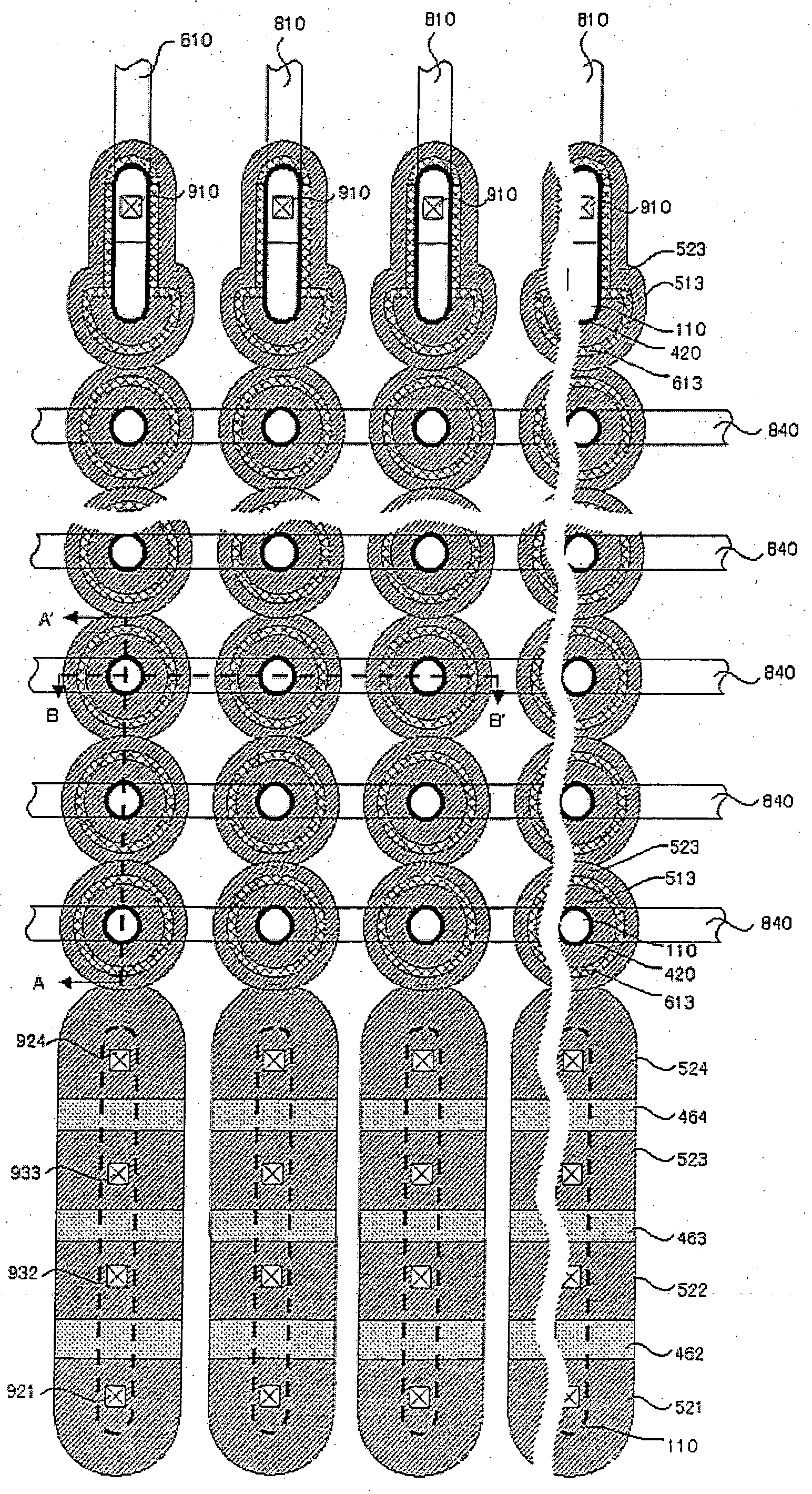
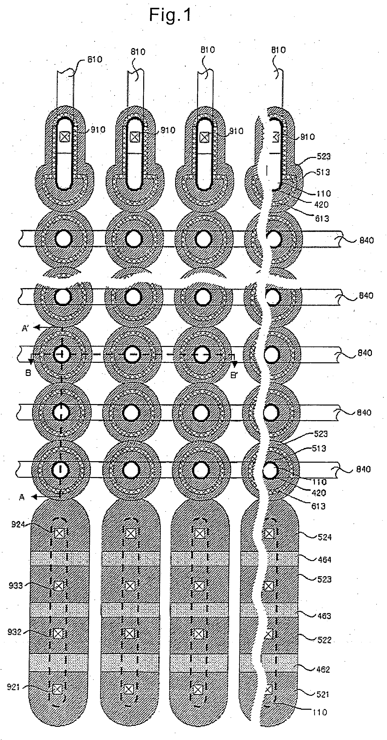
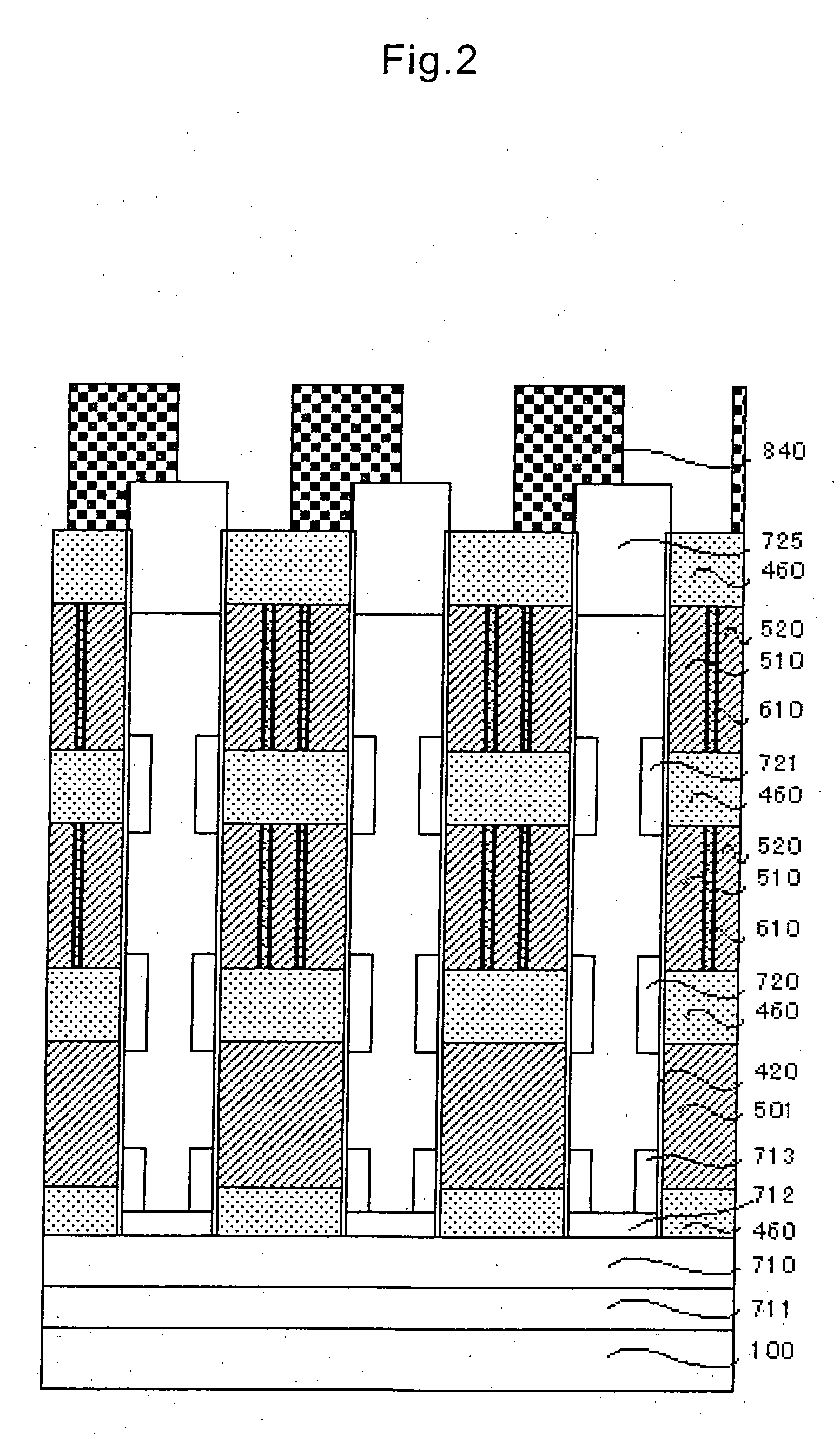
[0070]FIG. 1 is a plan view of a memory cell unit array including memory cell units arranged in a matrix configuration according to a first embodiment. FIG. 2 is a sectional view of one example of the memory cell unit array taken along a line A-A′ in FIG. 1. In this embodiment, the memory cell units are respectively provided in association with column-shaped semiconductor layers 110 arranged in a matrix configuration on a p-type silicon substrate 100. The memory cell units each include a selection transistor having a selection gate 501 provided on a lower portion of the column-shaped semiconductor layer 110, and two memory cell transistors provided above the selection transistor and connected in series along the column-shaped semiconductor layer. The number of the memory cells provided in each of the memory cell units is not limited to two, but it is merely necessary to provide plural memory cells in the memory cell unit. For example, three memory cells may be...

second embodiment

[0079] Second Embodiment

[0080] An explanation will hereinafter be given to a memory cell array driving method according to the present invention. FIG. 10 is an equivalent circuit diagram of a memory cell unit to be driven by the driving method according to a second embodiment. The memory cell unit of FIG. 10 is an exemplary flash memory of a NAND memory cell type, which includes one or more memory cells (two memory cells M1, M2 in this embodiment) and two selection transistors N1, N2. FIG. 11 is a block diagram illustrating a memory cell unit array including a plurality of such NAND memory cell type flash memories arranged in a matrix configuration. FIG. 12 is an equivalent circuit diagram of the memory cell unit array.

[0081] As shown in FIGS. 11 and 12, the memory cell unit array includes NAND memory cell units Paa, Pab to Pac, Pad to be selected by selection gate lines SG1a, SG2a and control gate lines CG1a, CG2a, NADN memory cell units Pba, Pbb to Pbc, Pbd to be selected by sele...

third embodiment

[0099] Third Embodiment

[0100]FIG. 15 is an equivalent circuit diagram illustrating a memory cell unit including a single selection transistor according to a third embodiment. A memory cell unit array according to this embodiment has substantially the same construction as shown in FIG. 11. The memory cell unit is a flash memory of a type which includes one or more memory cells (two memory cells M3, M4 in this embodiment) and a single selection transistor N3. An explanation will be given to a driving method for this flash memory.

[0101] Writing Operation

[0102] Where electrons are to be injected into a charge storage layer 1 of the memory cell M3 in any one of selected memory cell units by a tunnel current for a writing operation, a high voltage VH1 is applied to a control gate 2, and a voltage VH2 (VH1>VH2) such as to prevent the writing is applied to a control gate 4. A voltage VH4 which is one half a writing prevention voltage VH5 to be applied to bit lines is applied to a selectio...


PUM


Abstract

A memory cell unit including: a semiconductor substrate having a source diffusion layer in at least a part of a surface thereof; a column-shaped semiconductor layer provided on the semiconductor substrate, and having a drain diffusion layer provided in an uppermost portion thereof and a first low concentration impurity diffusion layer provided in an entire bottom portion thereof; a memory cell arrangement which includes a plurality of memory cells provided in a peripheral wall of the column-shaped semiconductor layer and connected in series perpendicularly to the substrate, the memory cells each having a charge storage layer and a control gate; a second impurity diffusion layer provided at a lower end of the memory cell arrangement; and a selection transistor having a gate electrode provided around the peripheral wall of the column-shaped semiconductor layer and connecting the second impurity diffusion layer and the first impurity diffusion layer; wherein the first impurity diffusion layer extends into a part of a channel region provided in the peripheral wall of the column-shaped semiconductor layer in opposed relation to the gate electrode of the selection transistor.

Description

CROSS-REFERENCE TO RELATED APPLICATION [0001] This application is related to Japanese application No.2003-326466 filed on Sep. 18, 2003 whose priority is claimed under 35 USC §119, the disclosure of which is incorporated by reference in its entirety. BACKGROUND OF THE INVENTION [0002] 1. Field of the Invention [0003] The present invention relates to a memory cell unit, a nonvolatile semiconductor storage device including such a memory cell unit, and a memory cell array driving method. [0004] 2. Description of the Related Art [0005] Exemplary memory cells of a known EEPROM are of a MOS transistor structure, which includes a gate portion including a charge storage layer and a control gate and is adapted to inject electric charges into the charge storage layer and release the electric charges from the charge storage layer by utilizing a tunnel current. The memory cells each store data “0” and “1” on the basis of a difference in threshold voltage attributable to a difference in the char...

Claims


Application Information

Patent Timeline
Patent Type & Authority Applications(United States)
IPC IPC(8): G11C16/02G11C7/00G11C16/04H01L21/8247H01L27/115H01L29/788H01L29/792
CPCG11C16/0483H01L27/115H01L29/7926H01L29/7881H01L29/792H01L27/11556H10B41/27H10B69/00H10B41/41
Inventor MASUOKA, FUJIOSAKURABA, HIROSHIMATSUOKA, FUMIYOSHIUENO, SYOUNOSUKEMATSUYAMA, RYUSUKEHORII, SHINJITANIGAMI, TAKUJI
Owner SAMSUNG ELECTRONICS CO LTD
Why Eureka
Try Eureka