Semiconductor device and method of fabricating semiconductor device

a semiconductor and semiconductor technology, applied in the direction of polycrystalline material growth, polycrystalline material growth, chemically reactive gas, etc., can solve the problems of difficult establishment and maintenance, difficult to selectively grow crystals, and inconvenient mass production methods for selective growth of epitaxial growth layers

Inactive Publication Date: 2005-03-31
PANASONIC CORP
View PDF4 Cites 5 Cited by
  • Summary
  • Abstract
  • Description
  • Claims
  • Application Information

AI Technical Summary

Benefits of technology

[0024] An object of the present invention is to provide a semiconductor device in which the layer thickness of an epita

Problems solved by technology

Although it has been reported that an epitaxial layer 106 can be selectively formed by optimizing the kind of material gas and crystal growth conditions, such a selective crystal growth is practically difficult since conditions capable of forming the epitaxial layer 106 are difficult to establish and maintain.
Therefore, the method for selectively growing an epitaxial growth layer is not suitable for mass production.
However, in the conventional non-selective growth method, there has arisen a problem that the control of layer thickness of an Si epitaxial layer is technically difficult.
However, in this method, since the peripheral wall of the reaction chamber 201 is heated to a high temperature, a film is also formed on this peripheral wall and comes off when deposited to a certain extent, thereby causing the formation of particles.
It has been found out that the amount of heat emitted from the substrate depends largely on the material of the substrate surface and t

Method used


Image

  • Semiconductor device and method of fabricating semiconductor device
  • Semiconductor device and method of fabricating semiconductor device
  • Semiconductor device and method of fabricating semiconductor device

Examples


first embodiment

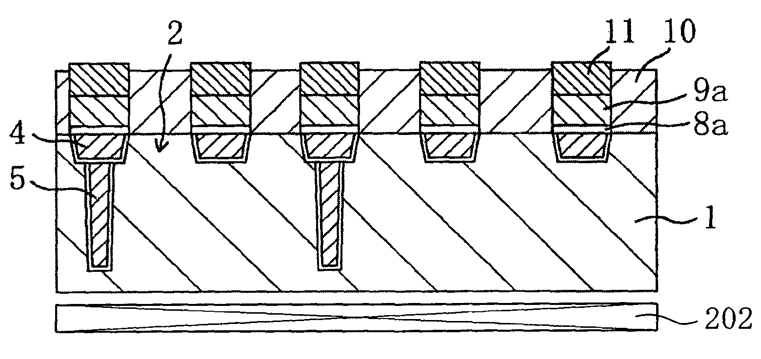
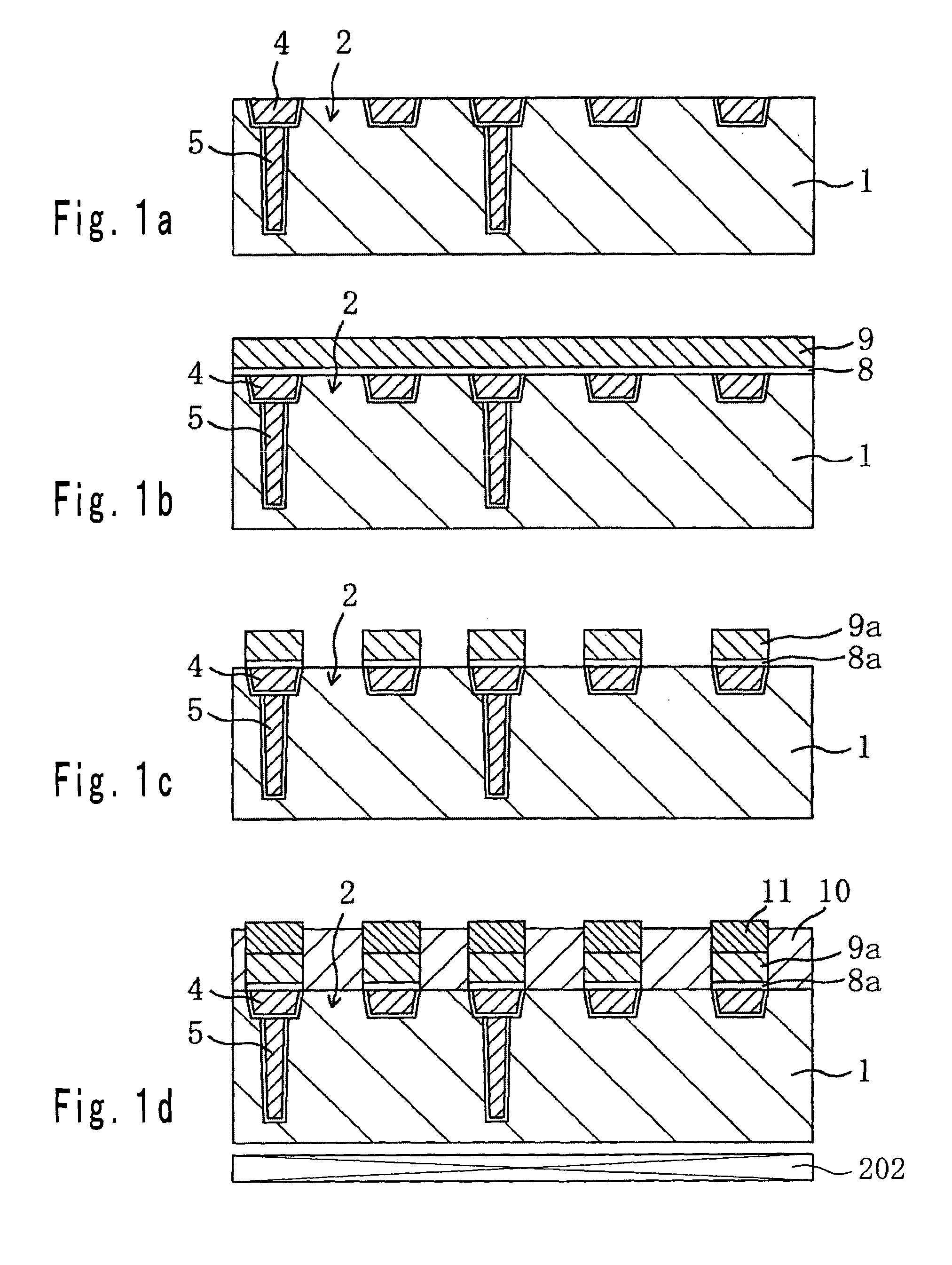
[0053]FIGS. 1a-1d are sectional views showing a method of fabricating a semiconductor device according to a first embodiment of the present invention.

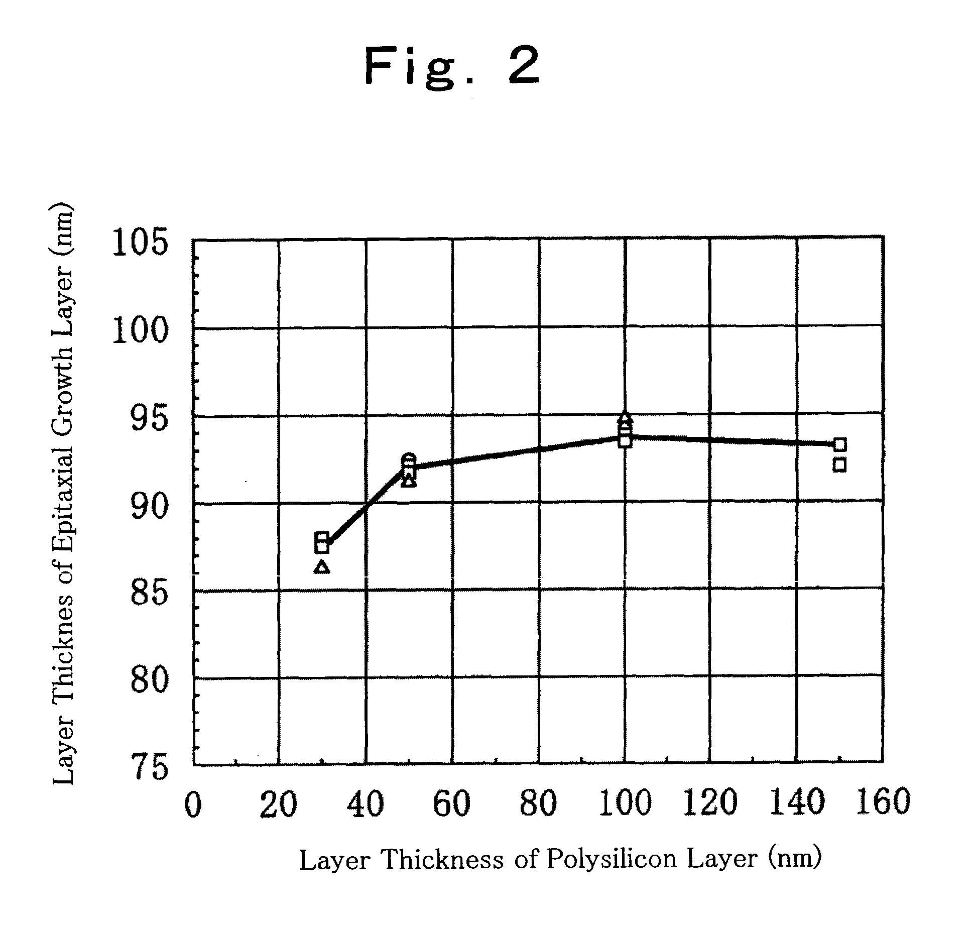
[0054] The present embodiment exemplifies a case where an SiGe epitaxial growth layer is made to grow on an Si substrate as a method of fabricating a semiconductor device. In the present embodiment, CVD was performed using a cold wall type shown in FIG. 10a. The opening area ratio of an active region 2 (a ratio of a total area of the active region 2 to a surface area of a substrate 1; this is substantially equal to the opening area ratio in a polysilicon layer 9a in the present embodiment) is on the order of 10%. Therefore, in FIGS. 1a-1d, an active region 2 is more exaggerated than a shallow trench isolation 4.

[0055] First, in a step shown in FIG. 1a, in the substrate 1 having the active region 2 made of Si crystal, the shallow trench isolation 4 where silicon oxide film is buried and a deep trench isolation 5 where undoped polysili...

second embodiment

[0073] In a second embodiment of the present invention, an example will be described in which the semiconductor device and the fabrication method thereof according to the first embodiment are applied to a bipolar transistor and a fabrication method thereof. More specifically, a bipolar transistor including an epitaxial growth layer and a polysilicon layer situated around and having a thickness of not less than approximately 50 nm and a fabrication method thereof will be described.

[0074] First of all, referring to FIG. 7b, a structure of the bipolar transistor according to the present embodiment will be described. FIG. 7b is a sectional view showing a structure of the bipolar transistor according to the present embodiment. An upper portion of an Si substrate 21 has a retrograde well 22 containing an n-type impurity such as P. And, the Si substrate 21 is provided with a collector layer 23, a shallow trench isolation 24 and a deep trench isolation 25 which serve as isolations surround...

third embodiment

[0101]FIG. 8 is a sectional view showing a structure of a bipolar transistor according to a third embodiment of the present invention. In FIG. 8, the same reference numerals as those in FIG. 7b denote the same or corresponding parts. It should be noted that a collector layer 23 is more exaggerated than a shallow trench isolation 24 in FIG. 8.

[0102] As shown in FIG. 8, in the third embodiment, the extrinsic base 38 is comprised of the polysilicon layer 29, the poly-SiGe layer 33, and the p+ polysilicon layer 36, whereas, in the present embodiment, the extrinsic base 38 is comprised of the polysilicon layer 29 and the poly-SiGe layer 33. According to the present embodiment, a second deposited oxide film 35 is formed in the step shown in FIG. 4b of the second embodiment. Then, the deposited oxide film 35 is patterned to have a predetermined shape, and an emitter opening portion 34 is formed in the deposited oxide film 35. Subsequently, an n+ polysilicon layer 40 is formed so as to fil...


PUM


Abstract

A method of fabricating a semiconductor device according to the present invention includes a step A of forming a polycrystalline or amorphous preliminary semiconductor layer on a surface of a substrate so as to have an opening portion and a step B of simultaneously forming an epitaxial growth layer on an exposed portion of a surface of the substrate through the opening portion and a non-epitaxial growth layer on the preliminary semiconductor layer using a CVD method while heating the substrate inside a reaction chamber by means of a heat source inside the reaction chamber, the epitaxial growth layer being made of single crystalline semiconductor, and the non-epitaxial growth layer being comprised of a polycrystalline or amorphous semiconductor layer.

Description

BACKGROUND OF THE INVENTION [0001] 1. Field of the Invention [0002] The present invention relates to a semiconductor device and a method of fabricating the semiconductor device, and more specifically to a hetero-bipolar transistor and a method of fabricating the hetero-bipolar transistor. [0003] 2. Description of the Related Art [0004] In these years, in order to improve the performance of Si devices, an epitaxial growth technology using in-situ doping has been adopted, in which a dopant source material is supplied onto an Si substrate together with an Si source material. With this technology, the thickness and dopant profile in the formed film can be controlled by in-situ doping in epitaxial growth with a high degree of accuracy during an epitaxial growth, and, therefore, it is possible to obtain high performance devices as compared to an ion implantation process technology. Improvement of the performance has also been realized by using quantum effects by epitaxially growing a mate...

Claims


Application Information

Patent Timeline
IPC IPC(8): H01L21/20H01L21/205H01L21/331
CPCH01L29/66242H01L21/02381H01L21/02639H01L21/0262H01L21/02532
Inventor SAITOH, TOHRUNOZAWA, KATSUYAKUBO, MINORUAOKI, SHIGETAKA
Owner PANASONIC CORP
Why Eureka
Try Eureka