Nitride-based semiconductor device

a technology of semiconductor devices and nitride, which is applied in the direction of semiconductor devices, nano-optics, electrical devices, etc., can solve the problems of increasing longitudinal serial resistance, increasing forward voltage, and deteriorating light emission efficiency, so as to improve optical power and optical efficiency.

Active Publication Date: 2005-03-31
SAMSUNG ELECTRONICS CO LTD
View PDF2 Cites 44 Cited by
  • Summary
  • Abstract
  • Description
  • Claims
  • Application Information

AI Technical Summary

Benefits of technology

[0017] The present invention has been made in view of the above mentioned technical problems, and an object of the invention is to provide a nitride-based semiconductor device in which an anti-diffusion film is formed at the interface of a quantum barrier layer with a quantum well layer in order to prevent an n type impurity from being diffused into the quantum well layer, so that it is possible to achieve an improvement in optical power and optical efficiency without degrading the optical characteristics of the quantum well layer.

Problems solved by technology

For this reason, in the case having the above mentioned MQW structure, there may be problems of an increase in longitudinal serial resistance caused by an increased layer thickness, and thus, an increase in forward voltage (Vf).
However, the above mentioned conventional schemes may cause a degradation in light emission efficiency because the n type impurity doped in the quantum barrier layers may be diffused into the quantum well layers.
Thus, the scheme of doping an n type impurity in quantum barrier layers may practically adversely affect the light emission efficiency and optical characteristics of the resultant LED structure.

Method used


Image

  • Nitride-based semiconductor device
  • Nitride-based semiconductor device
  • Nitride-based semiconductor device

Examples


example 1

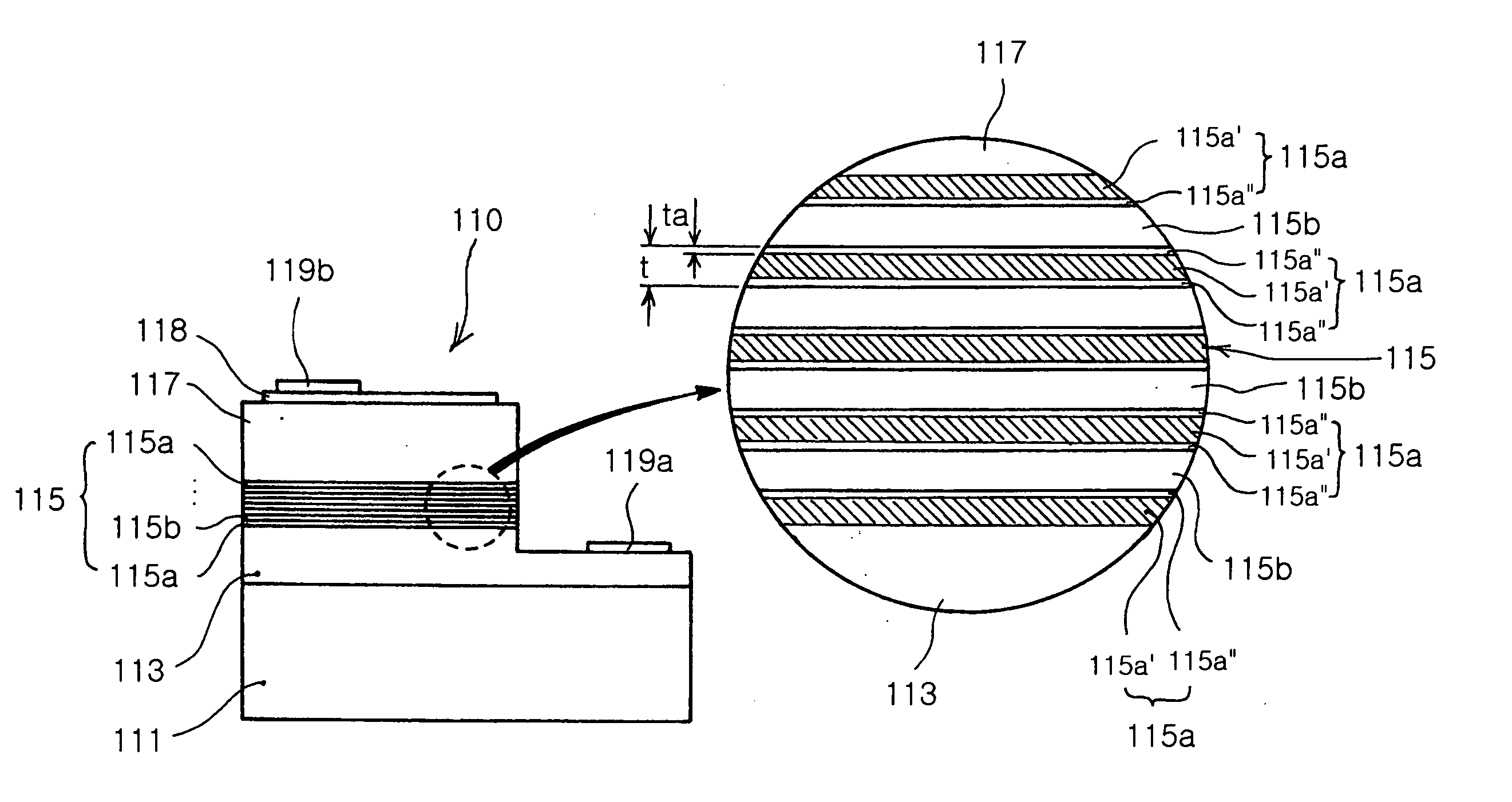
[0055] In this example, an LED was manufactured by sequentially depositing, over a sapphire substrate, an n type GaN semiconductor layer, an active layer having an MQW structure, and a p type GaN semiconductor layer, under the same deposition condition using an MOCVD process. The active layer having an MQW structure was formed to include five quantum well layers and six quantum barrier layers alternately laminated over one another. Each quantum well layer was made of an InGaN semiconductor layer having a thickness of 3 nm, whereas each quantum barrier layer was made of a GaN semiconductor layer having a thickness of 18 nm.

[0056] Also, each quantum barrier layer was formed to have anti-diffusion films having a thickness of 3 nm while being arranged at respective interfaces of the quantum barrier layer with the quantum well layers arranged adjacent thereto, similar to the structure of FIG. 3. The anti-diffusion films were not doped with any impurity intentionally. Each quantum barrie...

example 2

[0057] In this example, an LED was manufactured under the same condition as that in Example 1, except that although each quantum barrier layer included in the active layer had the same anti-diffusion film as that of Example 1, it was doped with Si in an amount of 0.48 nmol at its internal layer portion, so as to have an impurity concentration of 5×10¹⁶ / cm3.


PUM


Abstract

Disclosed is a nitride-based semiconductor device including a first nitride semiconductor layer doped with an n type impurity, an active layer formed on the first nitride semiconductor layer, the active layer including a plurality of quantum well layers and a plurality of quantum barrier layers alternately laminated over one another, at least one of the quantum layers being doped with the n type impurity, and a nitride semiconductor layer formed over the active layer, and doped with a p type impurity. The quantum barrier layer doped with the n type impurity includes an internal layer portion doped with the n type impurity, and an anti-diffusion film arranged at an interface of the quantum barrier layer with an adjacent one of the quantum well layers, the anti-diffusion film having an n type impurity concentration lower than that of the internal layer portion.

Description

BACKGROUND OF THE INVENTION [0001] 1. Field of the Invention [0002] The present invention relates to a nitride-based semiconductor device, and more particularly to a nitride-based semiconductor device for use in light emitting diodes, laser diodes, and the like, which has an improved active layer structure to achieve a reduction in operating voltage, so that it has an improved output efficiency. [0003] 2. Description of the Related Art [0004] Generally, nitride semiconductors are widely used in green or blue light emitting diodes (LEDs) adapted as a light source for full-color displays, image scanners, various signal systems, and optical communication appliances. In such an LED, its active layer generates light in accordance with the principle of electron-hole recombination, and emits the generated light. [0005] The active layer of such an LED may have a single quantum well (SQW) structure or a multiple quantum well (MQW) structure having a plurality of quantum well layers each havi...

Claims


Application Information

Patent Timeline
Patent Type & Authority Applications(United States)
IPC IPC(8): H01S5/20H01L29/15H01L29/20H01L33/06H01L33/32H01L33/36
CPCB82Y20/00H01L29/155H01L33/32H01L33/06H01L29/2003H01S5/20
Inventor KIM, SUN WOON
Owner SAMSUNG ELECTRONICS CO LTD
Why Eureka
Try Eureka