
CMOS imager for cellular applications and methods of using such

a cellular application and imager technology, applied in the field of systems and methods for detecting and/or transmitting images, can solve the problems of modulation of displayed images, flickering modulation, and inability to address various flicker situations, so as to reduce power consumption of imaging devices

Active Publication Date: 2005-03-31
TRANSCHIP ISRAEL
View PDF39 Cites 208 Cited by
  • Summary
  • Abstract
  • Description
  • Claims
  • Application Information

AI Technical Summary

Benefits of technology

Various aspects of the present invention include an imaging device with one or more of the following units: a control unit, a serial interface unit, a parallel interface unit, an imaging unit, and a translation unit. In some embodiments, flicker detection and / or correction functionality is incorporated. Additionally, in some embodiments, a built-in self test associated with various analog circuitry in the imaging device is included. Further, in some embodiments, systems and methods for reducing power consumption by various analog circuitry within the imaging device are included. Yet further, in some embodiments, a parallel to serial conversion unit and associated serial output interface are included. These and many other novel aspects of the present invention are provided in greater detail in the proceeding portions of this document.
One particular embodiment of the present invention provides an imaging device and methods for using such that provide for advanced testing ability. In one aspect, an imaging device includes a pixel array. The imaging device further includes a selector that is operable to select between an input derived from the pixel array and at least one reference input. Such selection between the input derived from the pixel array and the at least one reference input is based at least in part on a signal derived from a digital domain. Further, the imaging device includes an analog to digital converter that is operable to convert a signal derived from the selector to the digital domain. In some cases, such an embodiment provides an ability to verify, the functionality of analog circuitry within the imaging device using a digital tester.
Various embodiments of the present invention include a pixel with a charge evacuation mechanism for reducing noise evident at the output of the pixel. In one aspect, the pixel includes a reset element used in relation to charging a light sensitive element. The evacuation mechanism is used to dissipate charge build up about the reset element. Dissipation of the charge results in a reduction of noise at the output of the pixel. In particular embodiments, such a pixel and / or charge evacuation mechanism is implemented using complementary metal oxide semiconductor (“CMOS”), field effect transistor (“FET”) technology.

Problems solved by technology

In such cases, a modulation of the displayed image can result.
Such modulation appears as a flicker and can be very distracting.
Furthermore, such an approach is limited to reducing flicker in a limited number of pre-determined environments, and thus may not be able to address various flicker situations.
This is particularly problematic for mobile devices that are used in ever changing environments.
Further, a limited reservoir of power typically exists for mobile devices.
As such, power consuming imaging applications are often incompatible with mobile devices.
However, such approaches often are both expensive and can result in increased dimensions of a mobile device.
Providing such a test, and controlling for such variables can be costly and time consuming.
Further, such an approach tests the imaging device holistically, and is limited in its ability to identify sub-components of the imaging device which may have failed.

Method used


Image

  • CMOS imager for cellular applications and methods of using such
  • CMOS imager for cellular applications and methods of using such
  • CMOS imager for cellular applications and methods of using such

Examples


Embodiment Construction

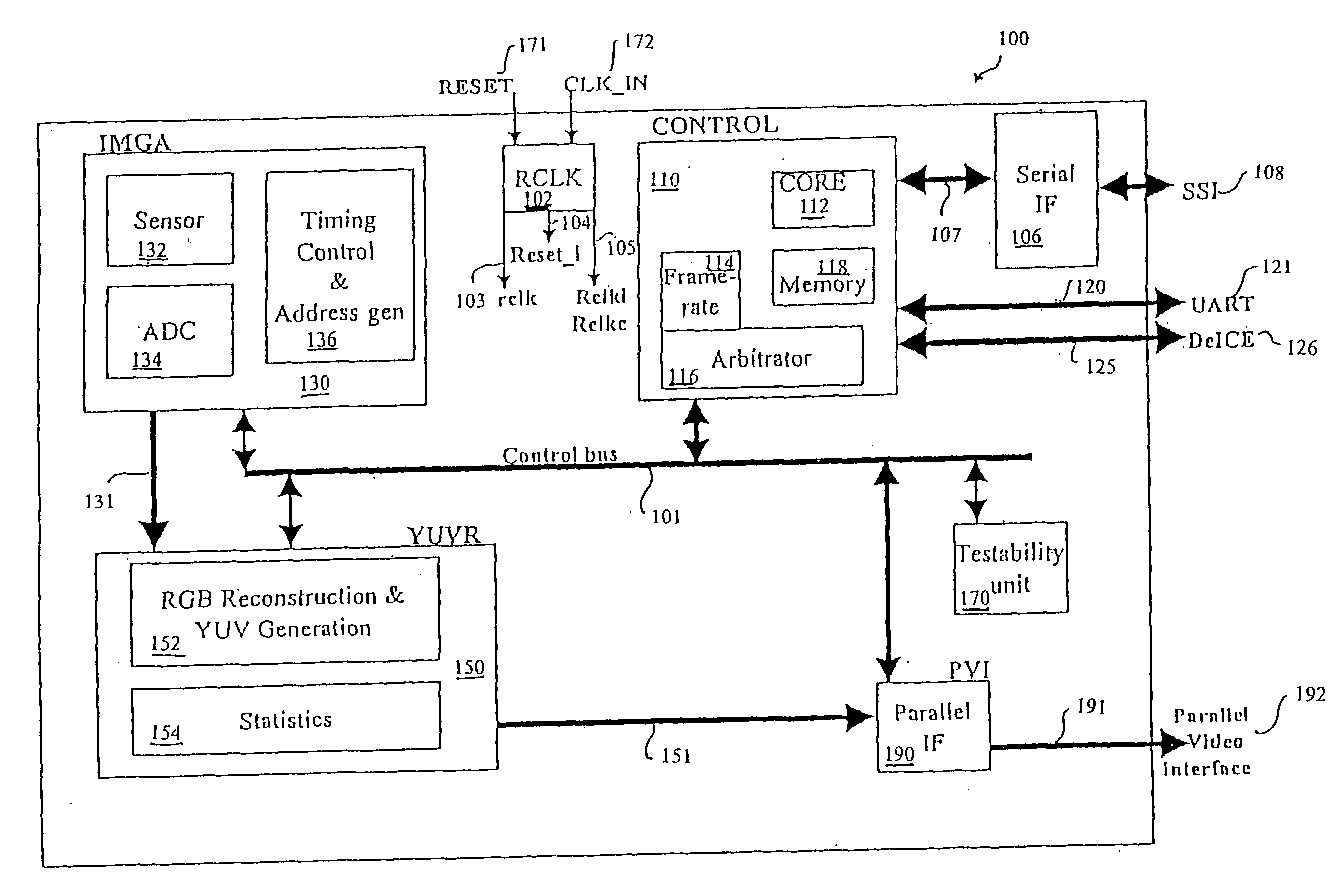
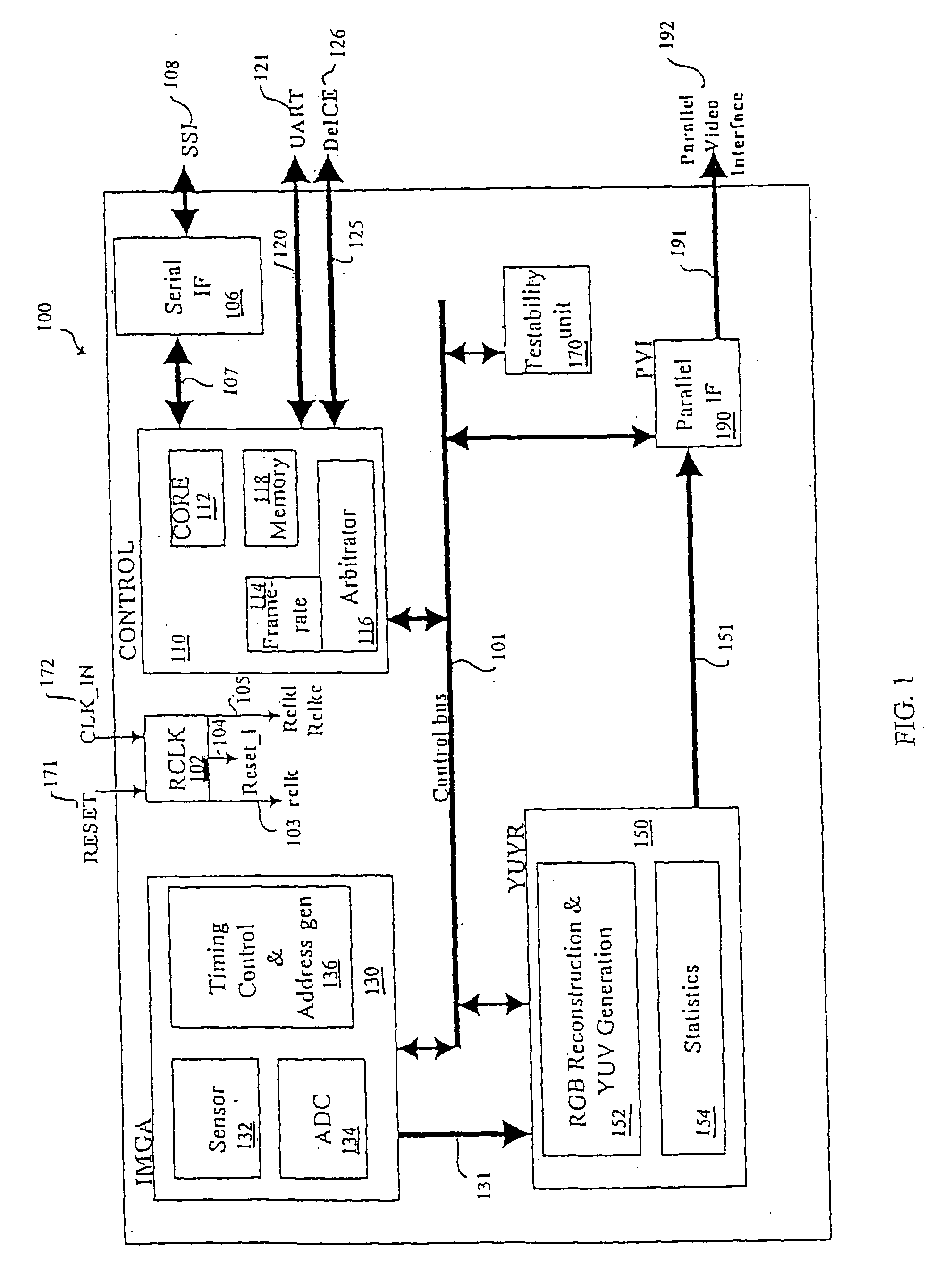
The present invention provides systems, devices, and methods for imaging. More particularly, the present invention provides devices and methods for capturing images, formatting the images, and / or transmitting the images via a cellular telephone network or other wireless network.

In one particular embodiment of the present invention, an imaging device including a CMOS sensor is provided. The imaging device includes an imager array, sensor timing control, and image processing algorithms integrated onto a single chip. Such an imaging device can produce CIF (i.e., 352×288) resolution image for still capture, and QCIF (i.e., 176×144) resolution image for video applications. In addition, the imaging device can perform various correction algorithms on a captured image to create a corrected YCrCb (4:2:2) image.

In an embodiment, the imager array is 384×316 physical pixels including 376×296 active pixels. The pixels can be mapped to a configurable size of output Bayer grid array (e.g., wi...


PUM


Abstract

Systems, methods and devices related to detecting and transmitting images. Imaging system and devices, as well as methods of using such that are provided herein include flicker detection and / or correction; and / or built-in self test (170) associated with various analog circuitry in the imaging devices; and / or power reduction ability; and / or pixels with charge evacuation functionality; and / or parallel to serial conversion (190) unit and associated serial output interface (106); and / or other advanced functionality.

Description

BACKGROUND OF THE INVENTION The present invention relates generally to systems and methods for detecting and / or transmitting images. More particularly, the present invention relates to detecting and transmitting images in relation to a cellular telephone. Image processors typically detect light reflected off of a subject, and convert the detected light to an electrical image. The electrical image is then sampled at a frequency that is the reciprocal of the integration time. In many cases, such a frequency is different from the frequency of light reflected off the subject. In such cases, a modulation of the displayed image can result. Such modulation appears as a flicker and can be very distracting. To overcome this problem, some image processors allow for manual selection between different integration times that allow a user to reduce the flicker. For example, where an image processor will be used in a 60 Hz and a 50 Hz lighting environment, a manual selection between an integrat...

Claims


Application Information

Patent Timeline
IPC IPC(8): H04N5/16H04N5/217H04N5/235H04N5/353H04N5/357H04N5/359H04N5/361H04N5/365H04N5/374H04N5/376H04N5/378H04N9/04H04N9/69H04N9/73H04N11/20H04N17/00
CPCH04N5/16H04N5/2178H04N5/23241H04N5/235H04N5/2351H04N5/2353H04N17/002H04N5/361H04N5/3765H04N5/378H04N9/69H04N9/73H04N11/20H04N5/2357H04N25/67H04N23/745H04N23/73H04N23/71H04N23/70H04N25/745H04N25/633H04N23/83H04N25/78H04N23/88H04N25/76H04N25/63H04N25/75
Inventor FRAENKEL, MIRIAMGALAMBOS, TIBERIU C.VORONOV, GERMANSHNAYDER, ALEXANDERFURMAN, BENELMAKIAS, YAIRANTSIFEROV, ILIA
Owner TRANSCHIP ISRAEL
Learn More