

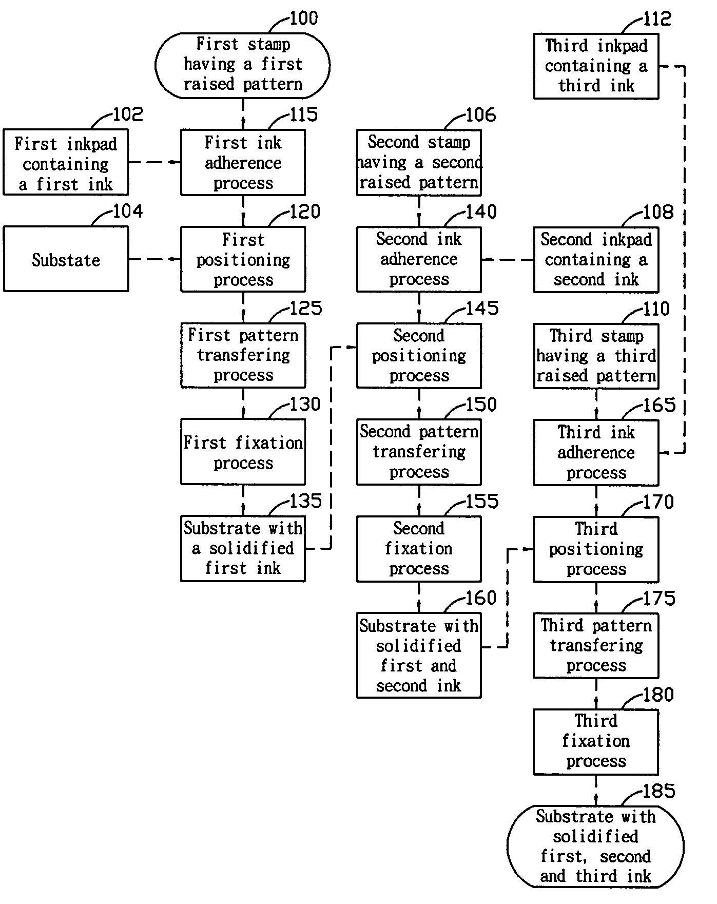
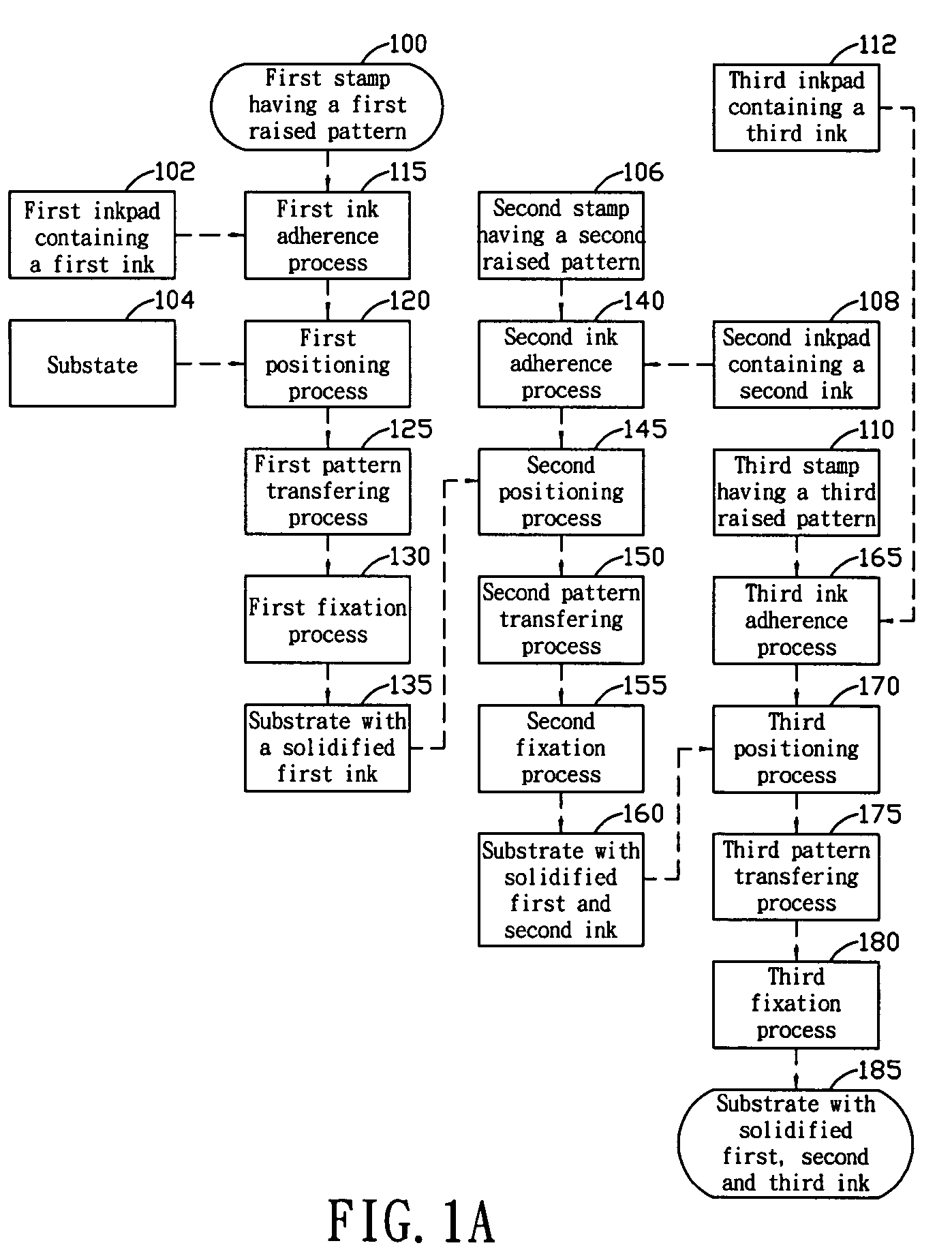
Micro-stamping method for photoelectric process
a photoelectric element and micro-stamping technology, applied in the field of micro-stamping method, can solve the problems of difficult to fabricate photoelectric elements with larger and more complicated patterns using this electro-deposition method, and the dyeing method is gradually disappearing, etc., to achieve the effect of high throughput and cost reduction
- Summary
- Abstract
- Description
- Claims
- Application Information
AI Technical Summary
Benefits of technology
Problems solved by technology
Method used
Image

Examples
Embodiment Construction
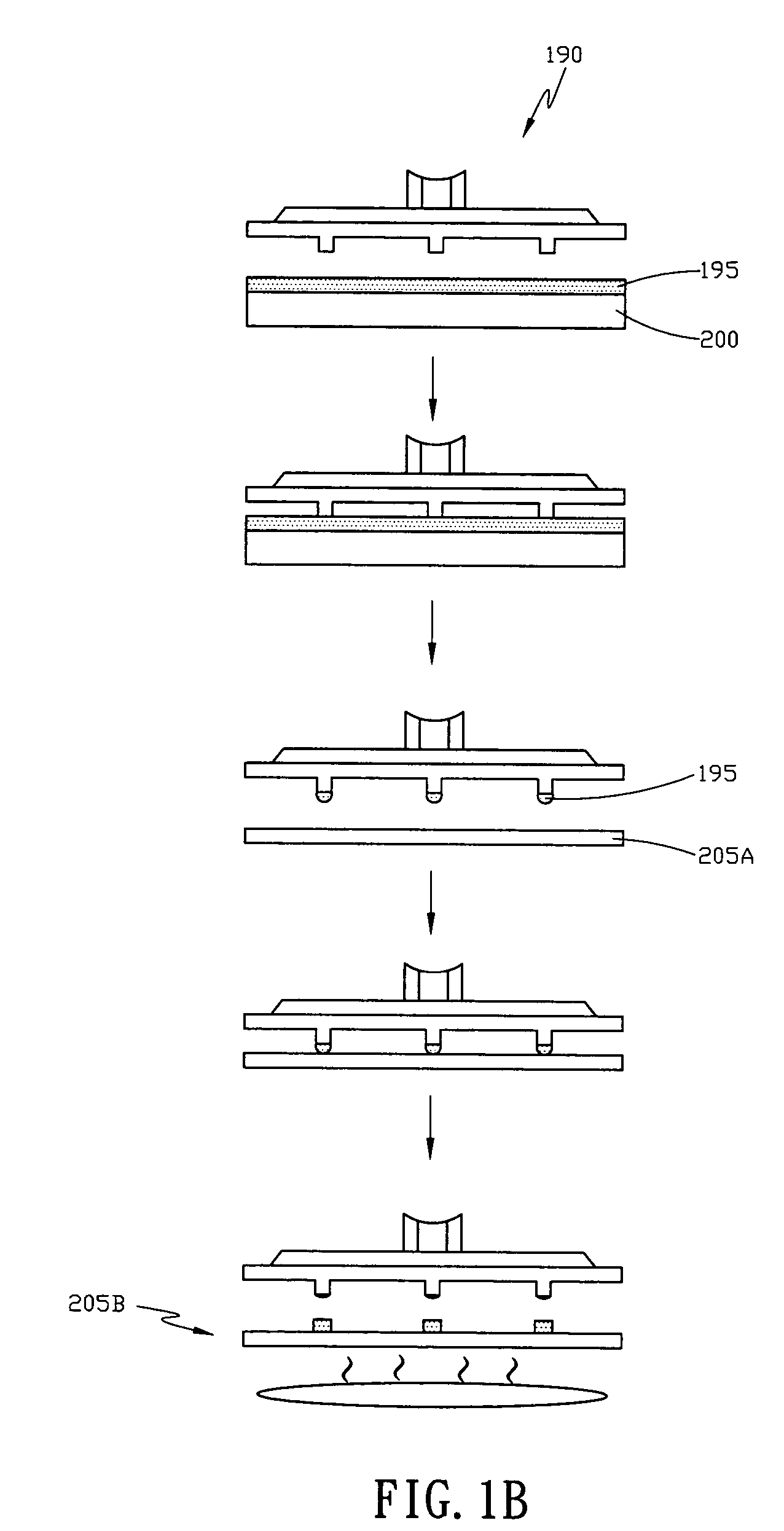
[0040] What is probed into in the invention is about a composite membrane for separating organic solvents and a method for forming the same. Detailed descriptions of the production, structure and elements will be provided in the following in order to make the invention thoroughly understood. Obviously, the application of the invention is not confined to specific details familiar to those who are skilled in the composite membrane for separating organic solvents. On the other hand, the common elements and procedures that are known to everyone are not described in details to avoid unnecessary limits of the invention. Some preferred embodiments of the present invention will now be described in greater detail in the following. However, it should be recognized that the present invention can be practiced in a wide range of other embodiments besides those explicitly described, that is, this invention can also be applied extensively to other embodiments, and the scope of the present inventio...
PUM
 Abstract
Description
Claims
Application Information