Nitride semiconductors on silicon substrate and method of manufacturing the same

a technology of nitride and compound semiconductor, which is applied in the direction of polycrystalline material growth, crystal growth process, chemically reactive gas growth, etc., can solve the problems of low electric conductivity and thermal conductivity, high cost, and inability to realize mass production of devices, so as to reduce the production of crystal defects, dislocation or cracks.

Inactive Publication Date: 2005-04-14
SAMSUNG ELECTRO MECHANICS CO LTD
View PDF12 Cites 46 Cited by
  • Summary
  • Abstract
  • Description
  • Claims
  • Application Information

AI Technical Summary

Benefits of technology

[0010] The present invention provides a nitride semiconductor in which the creation of crystal defects, dislocation or cracks is substantially decreased because a tensile stress, which can be generated between a Si substrate and a nitride semiconductor, is relaxed or removed, and a method of manufacturing the same.

Problems solved by technology

In conventional blue and green light emitting devices, substrates used in forming compound semiconductor layers thereon are sapphire or SiC substrates, not GaN substrates due to the difficulty of manufacturing GaN substrates.
However, the use of sapphire or SiC substrates results in high costs, low electric conductivity and thermal conductivity, and the mass production of devices is impossible to be realized because a large area cannot be grown.
That is, these substrates cannot be applied to MEMS, NEWS and micro-OEIC devices having photoelectric characteristics and electric-electron composite characteristics.
Despite this advantage, however, problems arise when a Group III nitride-based semiconductor layer, such as a GaN layer, is formed on the Si substrate.
Thus, crystal defects, dislocation, cracks and the like are created in a grown GaN layer.
In particular, the cracks cause the inner structure of crystals to be fragile, degrading device characteristics.
However, in these cases, the cracks cannot be prevented perfectly.
37, L966 (1998)) such as ELOG or PENDO has been used, the prevention of cracks is impossible, and the manufacturing process of a device using this method is complicated, resulting in high manufacturing costs.
The crystal defects ultimately result in the degradation of characteristics of completed semiconductor device.

Method used


Image

  • Nitride semiconductors on silicon substrate and method of manufacturing the same
  • Nitride semiconductors on silicon substrate and method of manufacturing the same
  • Nitride semiconductors on silicon substrate and method of manufacturing the same

Examples


Embodiment Construction

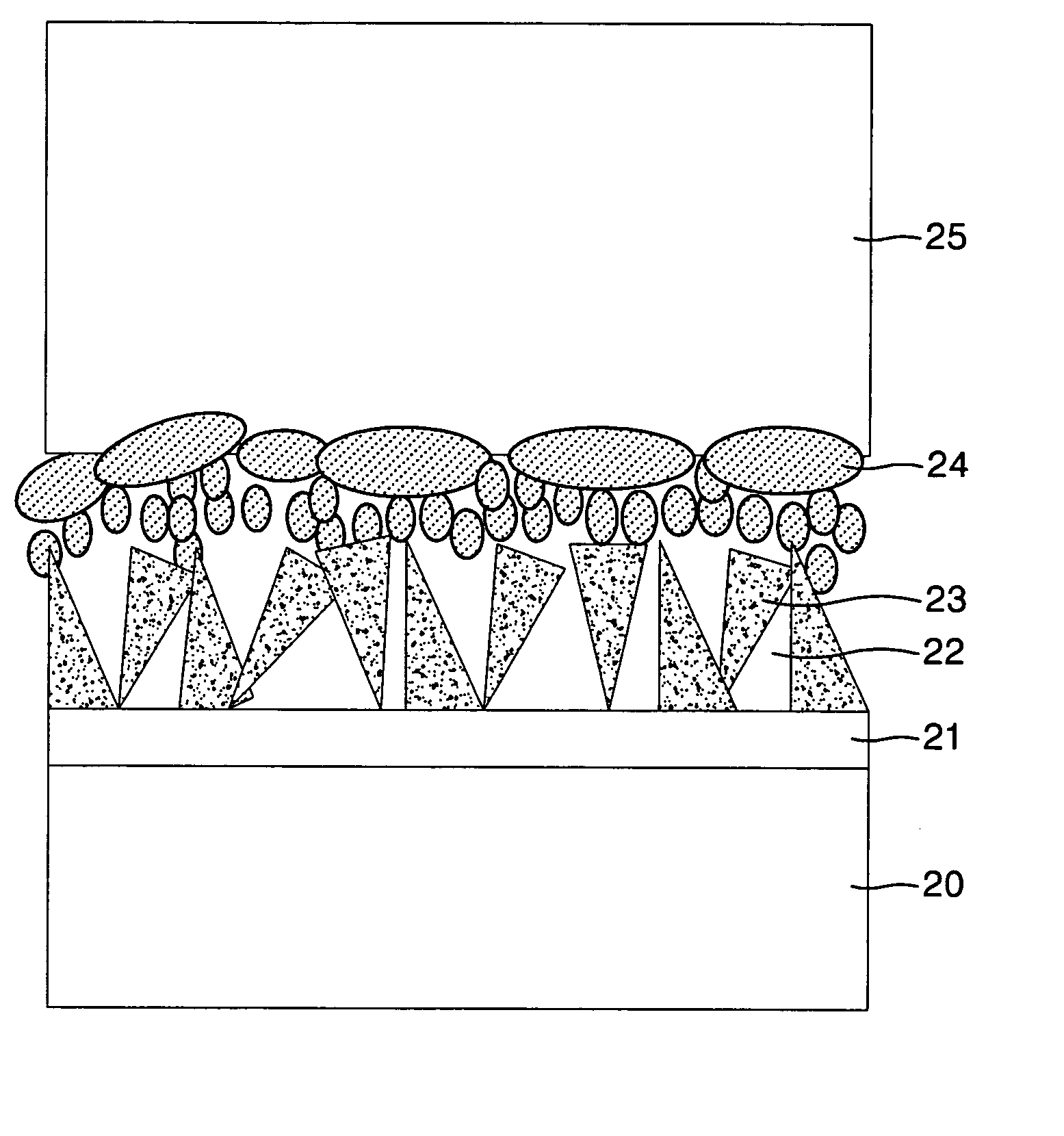
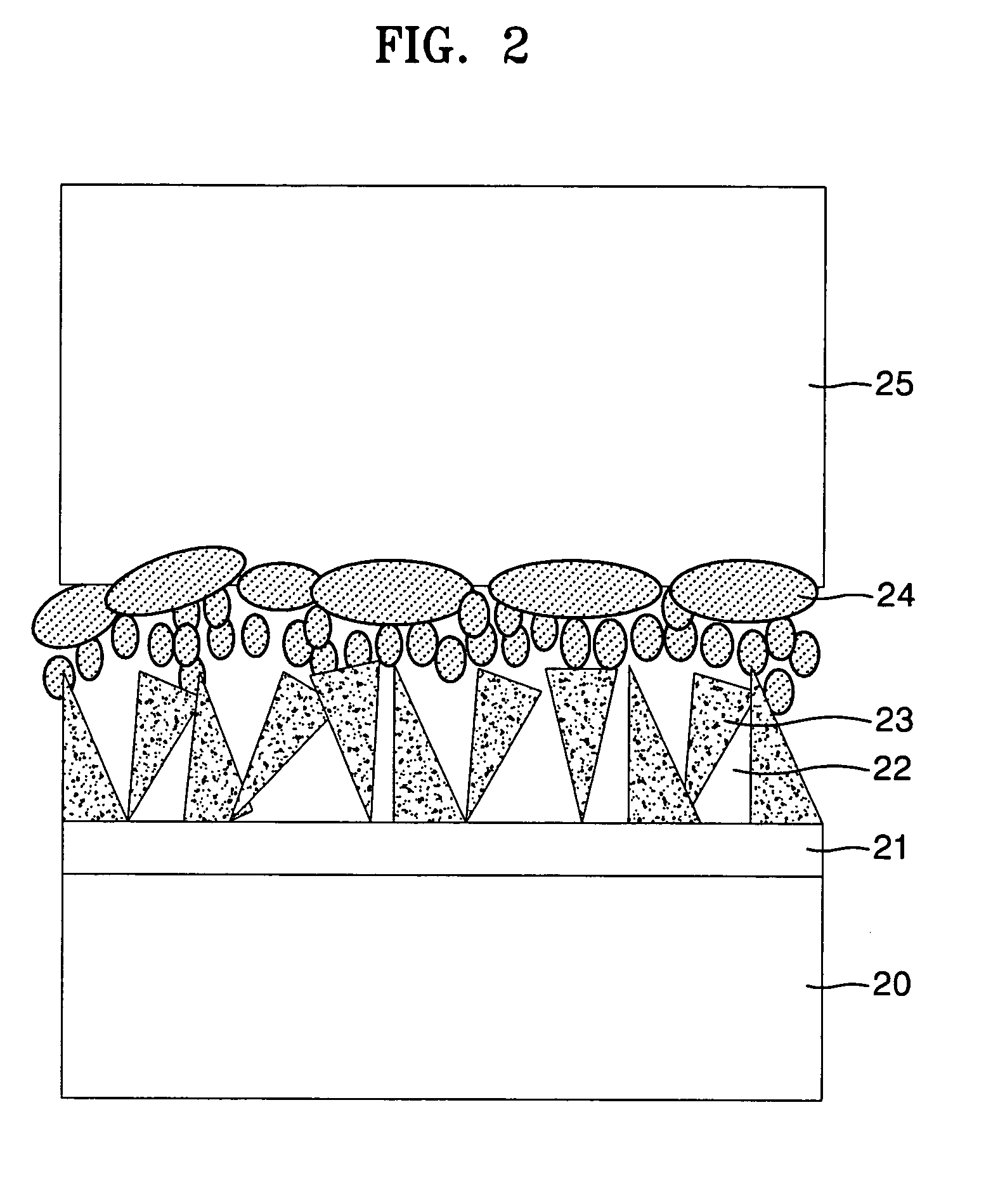
[0028]FIG. 2 is a cross-sectional view illustrating a nitride semiconductor grown on a Si substrate according to an embodiment of the present invention. Referring to FIG. 2, a buffer layer 21 is formed on a Si substrate, and an intermediate layer 23 having a plurality of voids 22 is formed on the buffer layer 21. A planarizing layer 24 is formed on the intermediate layer 23, and then a nitride compound 25 is formed on the planarizing layer 24.

[0029] The buffer layer 21 compensates for the wetting property because the nitride semiconductor material 25, for example GaN, is lack of the wetting property with respect to the Si substrate. The wetting property indicates the uniformity of an area density of a material formed from a base. When the wetting property is poor, planarization cannot be easily achieved because only a portion of the base can be grown. When a nitride-based compound such as GaN is formed on the Si substrate 20, the buffer layer 21 is interposed between those. The buf...


PUM

PropertyMeasurementUnit
thicknessaaaaaaaaaa
temperatureaaaaaaaaaa

Abstract

Provided is a nitride semiconductor formed on a Si substrate and a method of manufacturing the same. A buffer layer is formed on the silicon substrate, and an intermediate layer having voids is formed on the buffer layer. A planarizing layer is formed on the intermediate layer, and a nitride semiconductor layer is formed on the planarizing layer. Therefore, a nitride semiconductor in which the creation of crystal defects, dislocation or cracks is substantially decreased can be produced on a large scale at a low cost.

Description

BACKGROUND OF THE INVENTION [0001] This application claims the priority of Korean Patent Application No. 2003-70984, filed on Oct. 13, 2003, in the Korean Intellectual Property Office, the disclosure of which is incorporated herein in its entirety by reference. [0002] 1. Field of the Invention [0003] The present invention related to a nitride-based compound semiconductor and a method of growing a nitride compound semiconductor on a silicon substrate, and more particularly, to a nitride-based compound semiconductor formed on a silicon substrate without lattice defects and cracks because of an intermediate layer between the silicon substrate and a nitride-based compound semiconductor layer, and a method of manufacturing the same. [0004] 2. Description of the Related Art [0005] In conventional blue and green light emitting devices, substrates used in forming compound semiconductor layers thereon are sapphire or SiC substrates, not GaN substrates due to the difficulty of manufacturing G...

Claims


Application Information

Patent Timeline
Patent Type & Authority Applications(United States)
IPC IPC(8): C30B25/18C23C16/34C30B29/40H01L21/20H01L21/205H01L29/20H01L33/12H01L33/32H01L33/34
CPCC30B25/18C30B29/40H01L21/02381H01L21/02458H01L33/007H01L21/02513H01L21/0254H01L29/2003H01L21/02505
Inventor YOON, SUK-HOLEE, CHEUL-ROLEE, JEONG-WOOKLEE, SUNG-SOOK
Owner SAMSUNG ELECTRO MECHANICS CO LTD
Why Eureka
Try Eureka