Thin film for optical applications, light-emitting structure using the same and the fabrication method thereof

a technology of thin film and optical amplifier, applied in the direction of cladding optical fibre, optical waveguide light guide, active medium material, etc., can solve the problems of low luminous efficiency, low luminous efficiency of conventional rare earth-doped semiconductor, and high luminous efficiency of silica-based thin film, etc., to achieve high luminous efficiency and high excitation cross section

Inactive Publication Date: 2005-04-14
LUXPERT TECH
View PDF4 Cites 29 Cited by
  • Summary
  • Abstract
  • Description
  • Claims
  • Application Information

AI Technical Summary

Benefits of technology

[0021] Therefore, a new thin film structure for practical application can be accomplished, which has the high luminous efficiency of the rare earth element similar to the silica-based thin film as well as the high excitation cross section of the rare earth element similar to the semiconductor thin film.

Problems solved by technology

In particular, it is does not offer significant advantages in terms of cost, performance and potential for future development over optical amplifiers based on optical fibers.
For this reason, a conventional rare earth-doped semiconductor has the very low luminous efficiency.
In summary, the silica-based thin film has the high luminous efficiency but the very low excitation efficiency, while the semiconductor thin film has the high excitation efficiency but the very low luminous efficiency.
However, this model is only conceptual and has not been practically applied.

Method used


Image

  • Thin film for optical applications, light-emitting structure using the same and the fabrication method thereof
  • Thin film for optical applications, light-emitting structure using the same and the fabrication method thereof
  • Thin film for optical applications, light-emitting structure using the same and the fabrication method thereof

Examples


first embodiment

[0032] First Embodiment

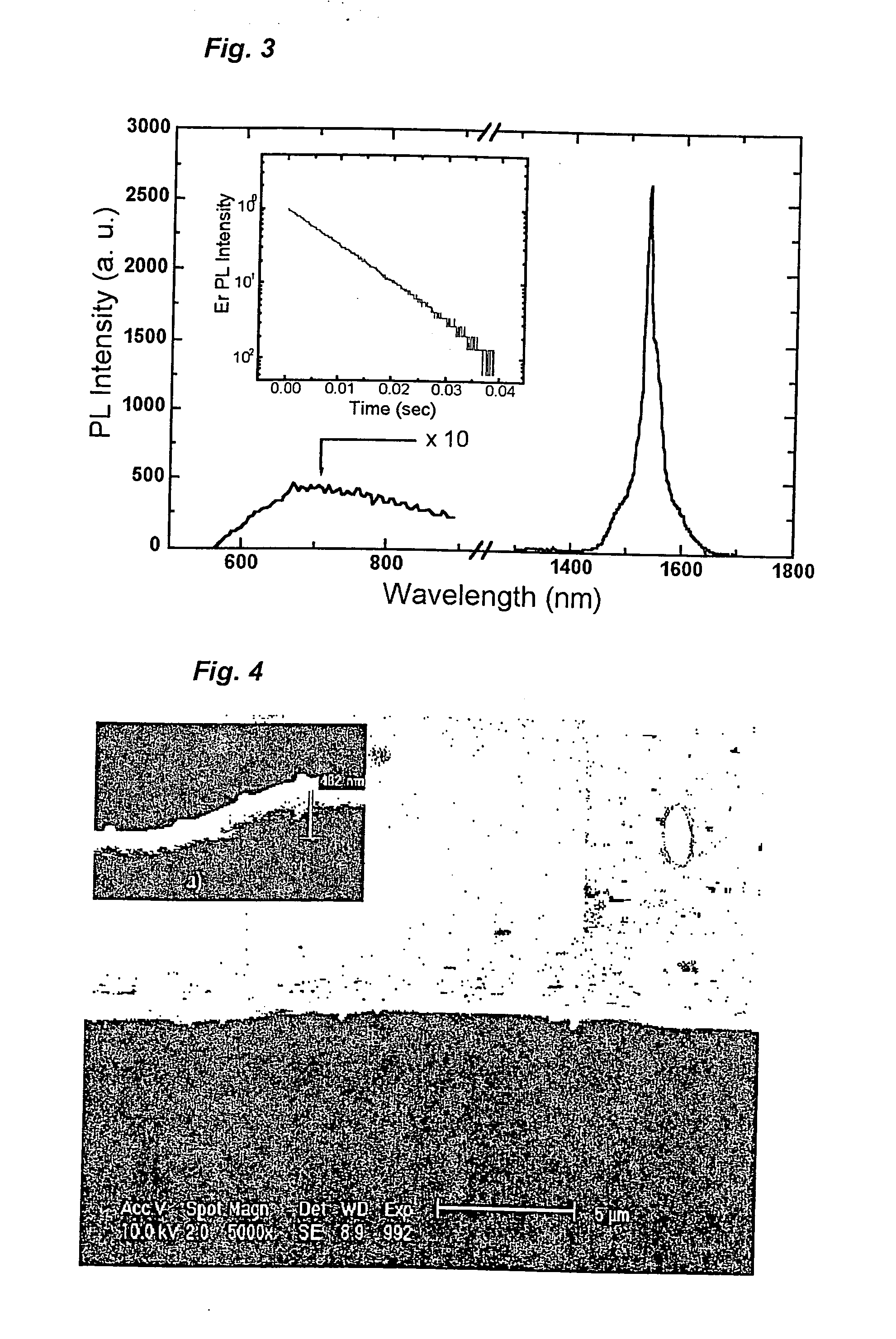
[0033]FIG. 3 is a graph showing the photoluminescence spectrum of a silica thin film for optical devices at room temperature according to the first embodiment of the present invention. The thin film comprising 35 atomic % of silicon, 65 atomic % of oxygen and 0.04 atomic % of erbium was chemical vapor deposited and heated at 1,000° C. for 5 minutes. As shown in FIG. 3, a luminescence peak of a silicon nanocluster was observed around 700 nm. The relationship between the position of the luminescence peak of the silicon nanocluster and the size of the silicon nanocluster is already known in the art. Based on this result, the average size of the silicon nanocluster in the thin film was calculated as 2 nm. In this case, the concentration of the silicon nanocluster was 7×1018 cm−3 and the concentration ratio of the doped erbium to the silicon nanocluster was 3. That is, it can be said that the thin film of FIG. 3 is manufactured according to the method of the presen...

second embodiment

[0047] Second Embodiment

[0048] In case of a silica or silica-based thin film which is co-doped with a silicon nanocluster and rare earth atoms, the rare earth atoms are excited through an electron-hole recombination formed in the silicon nanocluster regardless of the absorption band of the rare earth element. In this regard, in accordance with the second embodiment of the present invention, in case of doping various types of the rare earth elements on one thin film, it is possible to generate luminescence of various wavebands using one pump light source. FIG. 6 shows the photoluminescence spectra of silica thin films for optical devices doped with erbium and / or thulium. A pump light source of 488 nm wavelength was used alone. In FIG. 6, a solid line represents the thin film which is co-doped with erbium and thulium, a long dotted line represents the thin film which is doped with a high concentration of erbium, a short dotted line represents the thin film which is doped with a low co...

third embodiment

[0049] Third Embodiment

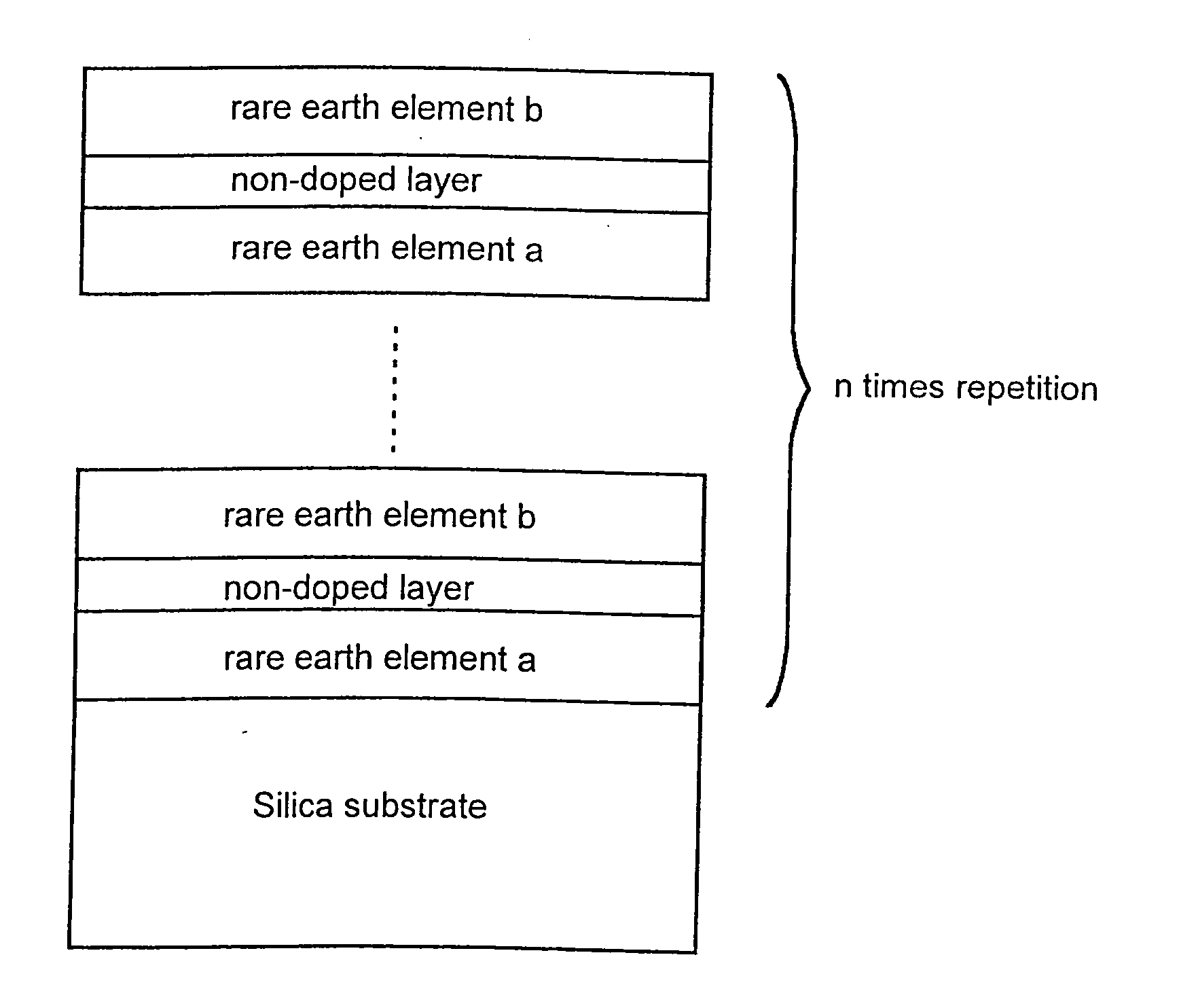
[0050] In case of using two types of rare earth elements according to the second embodiment of the present invention, these rare earth elements may interact with each other, thereby lowering the luminous efficiency. In order to solve this problem, it is necessary to dope the two types of rare earth elements on multiple silica layers in a manner such that one silica layer is doped with one type of a rare earth element (see FIG. 7a). Preferably, as shown in FIG. 7b, a non-doped silica layer can be sandwiched between the two types of rare earth elements. As a result, the two types of rare earth elements can be entirely prevented from interacting with each other. In this case, it is preferable to limit the thickness of each layer to 10 nm or less to ensure total uniformity of the thin film. FIGS. 7a and 7b are schematic cross sectional views showing the aforementioned thin film structures. It is understood that doping with two or more types of rare earth elements ...


PUM

PropertyMeasurementUnit
sizeaaaaaaaaaa
thicknessaaaaaaaaaa
pressureaaaaaaaaaa

Abstract

Thin film for optical applications, light-emitting structure using the same and the fabrication method thereof are disclosed. The present invention provides a silica or silica-related thin film for optical applications in which silicon nanoclusters and rare earth elements are co-doped. The average size of the silicon nanoclusters is less than 3 nm and the concentration of the rare earth elements is less than 0.1 atomic %. The ratio of the rare earth element concentration to that of silicon nanoclusters is controlled to range from 1 to 10 in the thin film. The thin film emits light by exciting the rare earth elements through electron-hole recombinations in the silicon nanoclusters. According to the present invention, the conditions such as the size and concentration of the silicon nanoclusters, the concentration of the rare earth element, and their concentration ratio are specifically optimized to fabricate optical devices with better performance.

Description

TECHNICAL FIELD [0001] The present invention relates to a silica or silica-based thin film and a method for manufacturing the same, and more particularly to a silica or silica-based thin films which are co-doped with rare earth atoms and silicon nanoclusters, as well as a method for manufacturing the same. Therefore, the excitation efficiency of the rare earth atoms is improved, resulting in efficient application of the thin film for optical devices. BACKGROUND ART [0002] Recently, a silica or silica-based thin film that is doped with rare earth atoms has widely been used to manufacture a waveguide amplifier. However, it is essentially similar to a silica or silica-based optical fiber that is doped with rare earth atoms. Furthermore, because the excitation cross section of the rare earth atoms is very low, on the level of 4×10⁻²¹ cm2, a high-priced laser for exciting the rare earth element and a WDM structure for dividing a signal light and a pump light are required. Such a waveguid...

Claims


Application Information

Patent Timeline
Patent Type & Authority Applications(United States)
IPC IPC(8): B82Y20/00G02B6/02H01S3/063H01S3/09H01S3/16H01S3/06
CPCH01S3/0632H01S3/09H01S3/169H01S3/1628H01S3/1608G02B6/02B82Y20/00
Inventor SHIN, JUNG-HOONSEO, SE-YOUNGHAN, HAK-SEUNG
Owner LUXPERT TECH
Why Eureka
Try Eureka