Semiconductor device and manufacturing method thereof

a technology of semiconductor devices and manufacturing methods, applied in semiconductor devices, electrical devices, transistors, etc., can solve the problems of excessive etching of contact holes, difficult decrease of the thickness of etching resistance films, and “aperture defects”, so as to suppress “aperture defects” and ensure process tolerance of shorts

Inactive Publication Date: 2005-04-14
RENESAS ELECTRONICS CORP
View PDF3 Cites 16 Cited by
  • Summary
  • Abstract
  • Description
  • Claims
  • Application Information

AI Technical Summary

Benefits of technology

[0016] The present invention is made to solve the problems as described above. An object of the present invention is to provide a semiconductor device allowing significant enlargement of a margin in a photolithographic p

Problems solved by technology

For design rules of at most 0.13 μm having an extremely narrow space between gate electrodes, a problem of an “aperture defect”, or a problem of difficulty in ensuring a process tolerance of an electrical “short” of the gate electrode and the polycrystal silicon film occurs in the above-described background art because of a microloading effect caused by a difference in hole diameters of the bit line contact and the storage node contact.
Therefore, when the etching is performed in a condition suitable for the contact hole having a larger hole diameter, the etching proceeds insufficiently in the contact hole of the smaller hole diameter, resulting in the “aperture defect”.
On th

Method used


Image

  • Semiconductor device and manufacturing method thereof
  • Semiconductor device and manufacturing method thereof
  • Semiconductor device and manufacturing method thereof

Examples


first embodiment

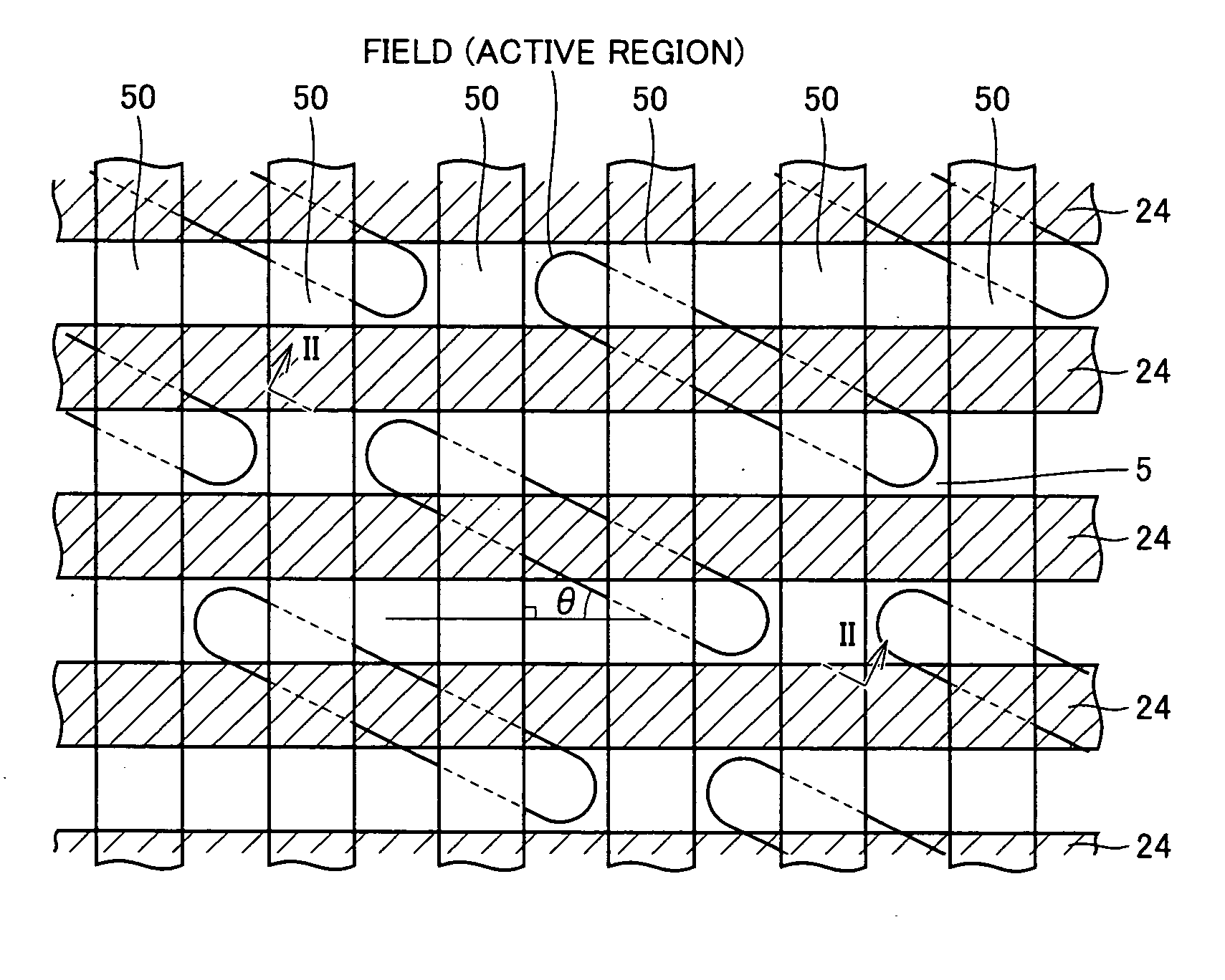
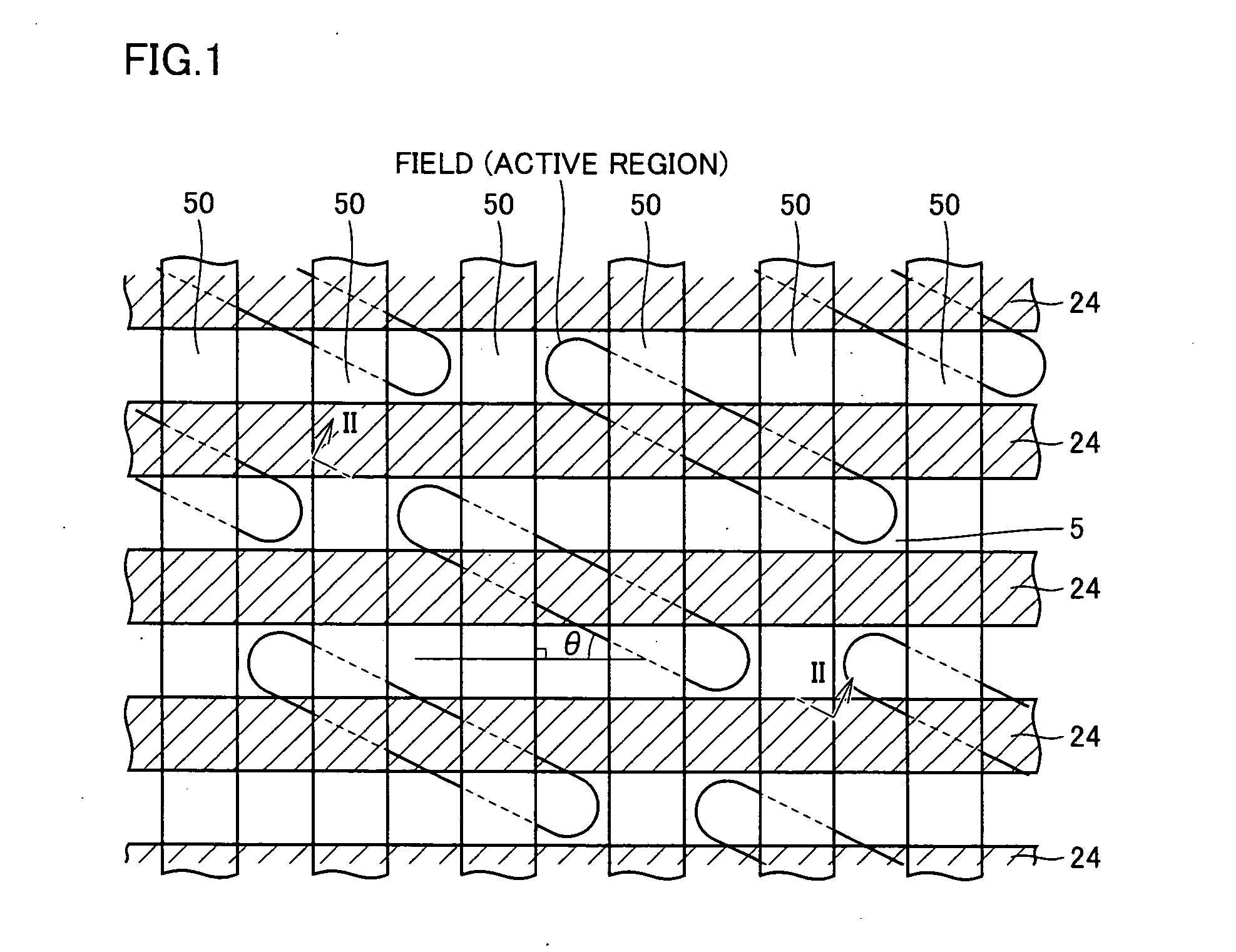
[0031] Referring mainly to FIG. 1, in a memory cell array of a DRAM, for example, each of a plurality of word lines (gate electrode layers) 50 and each of a plurality of bit lines 24 are arranged perpendicular to each other. A memory cell is arranged near an intersecting portion of each word line 50 and each bit line 24. A memory cell transistor is formed in an active region (field). A plurality of such active regions are arranged.

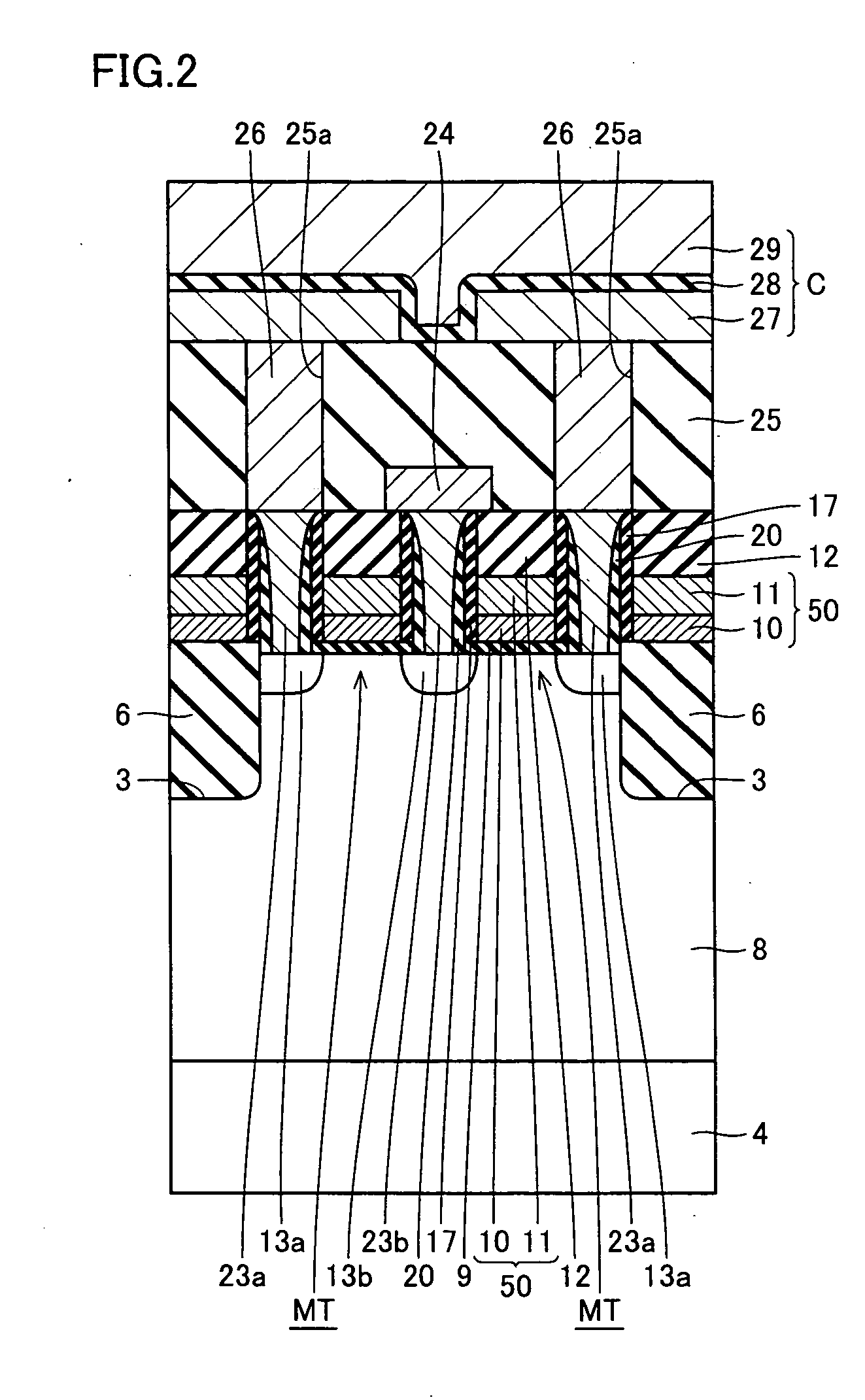
[0032] Referring mainly to FIG. 2, each of the plurality of active regions is surrounded with an element isolation structure on a surface of a semiconductor substrate 4 formed with, for example, a silicon substrate. The element isolation structure is formed with, for example, an STI (Shallow Trench Isolation) structure. The STI structure has a shallow trench 3 formed on a surface of semiconductor substrate 4 and an embedded insulation layer (which is, for example, a silicon oxide film) 6 embedded in shallow trench 3.

[0033] The memory cell has a memory tr...

second embodiment

[0078] Though band-shaped opening pattern 22a in the first embodiment is non-linear and has uneven width, opening pattern 22a having a uniform width may be formed. As opening pattern 22a with a uniform width, a linear band-shaped opening pattern 22a as shown in a plan view of FIG. 26 may be formed. As a result, a memory cell array of the DRAM having a plane layout as shown in FIG. 27 is formed. The capacitor is not shown in FIG. 27.

[0079] As a manufacturing method and a construction of this embodiment are similar to those in the first embodiment except for the aforementioned point, similar elements are indicated by the same reference characters and descriptions thereof will not be repeated here.

third embodiment

[0080] In the steps shown in FIGS. 17-19 in the first embodiment, planarization is performed by the CMP using cap film (hard mask layer) 12 as a stopper to make the upper surface of each of plug conductive layers 23a, 23b and the upper surface of cap film (hard mask layer) 12 parallel to the surface of silicon substrate 4. Planarization by the CMP, however, may be performed after dry etching is performed following the step of FIG. 17 or 18.


PUM


Abstract

A semiconductor device includes a silicon substrate having an active region, a memory transistor having a pair of source/drain regions and a gate electrode layer, a hard mask layer on the gate electrode layer having a plane pattern shape identical with that of the gate electrode layer, and plug conductive layers each electrically connected to each of the pair of source/drain regions. An extending direction of the active region is not perpendicular to that of the gate electrode layer, but is oblique. Upper surfaces of the hard mask layer and each of the plug conductive layers form substantially an identical plane. This can attain a semiconductor device allowing significant enlargement of a margin in a photolithographic process, suppression of an “aperture defect” as well as ensuring of a process tolerance of a “short” by decreasing a microloading effect, and decrease in a contact resistance, and a manufacturing method thereof.

Description

BACKGROUND OF THE INVENTION [0001] 1. Field of the Invention [0002] The present invention relates to a semiconductor device and a manufacturing method thereof. More specifically, the present invention relates to a semiconductor device having a self-aligned contact structure and a manufacturing method thereof. [0003] 2. Description of the Background Art [0004] As a degree of integration of a semiconductor device increases, a width of a wiring decreases and a space between the wirings also decreases. When a contact hole connecting upper and lower wirings is formed, the contact hole must be formed with a hole diameter smaller than a width of the space between adjacent wirings. That is, a hole diameter C of the contact hole required for design rules of 0.25 μm for the space between the adjacent wirings will be C≦0.25−f(α,β) μm, considering overlay accuracy (=α) and dimensional accuracy (=β) in a photolithographic processing step, which exceeds a limit of size reduction depending on a wa...

Claims


Application Information

Patent Timeline
IPC IPC(8): H01L21/768H01L21/8242H01L21/28H01L27/02H01L27/108H01L29/94
CPCH01L27/0207H01L27/10814H01L27/10894H01L27/10888H01L27/10855H10B12/315H10B12/0335H10B12/485H10B12/09
Inventor SHIRATAKE, SHIGERU
Owner RENESAS ELECTRONICS CORP
Why Eureka
Try Eureka