

Process for producing semiconductor device and semiconductor device
- Summary
- Abstract
- Description
- Claims
- Application Information
AI Technical Summary
Benefits of technology
Problems solved by technology
Method used
Image

Examples
first embodiment
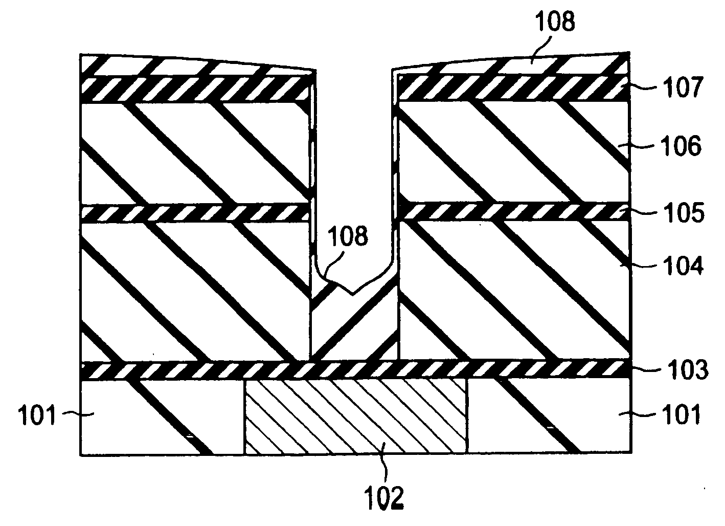
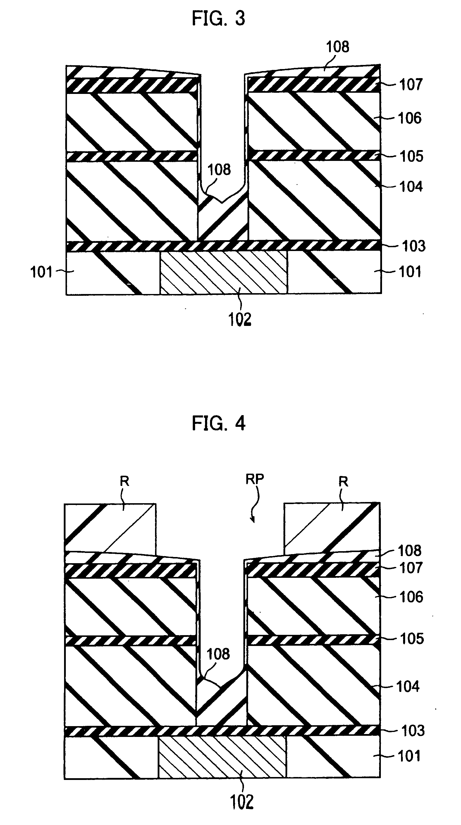
[0050]FIG. 9 is a sectional view of a wiring structure of a semiconductor device according to an embodiment of the present invention. Here, the case of further forming on a wiring layer a wiring pattern of a dual damascene structure wherein a via hole and a wiring layer are integrated will be explained as an example.
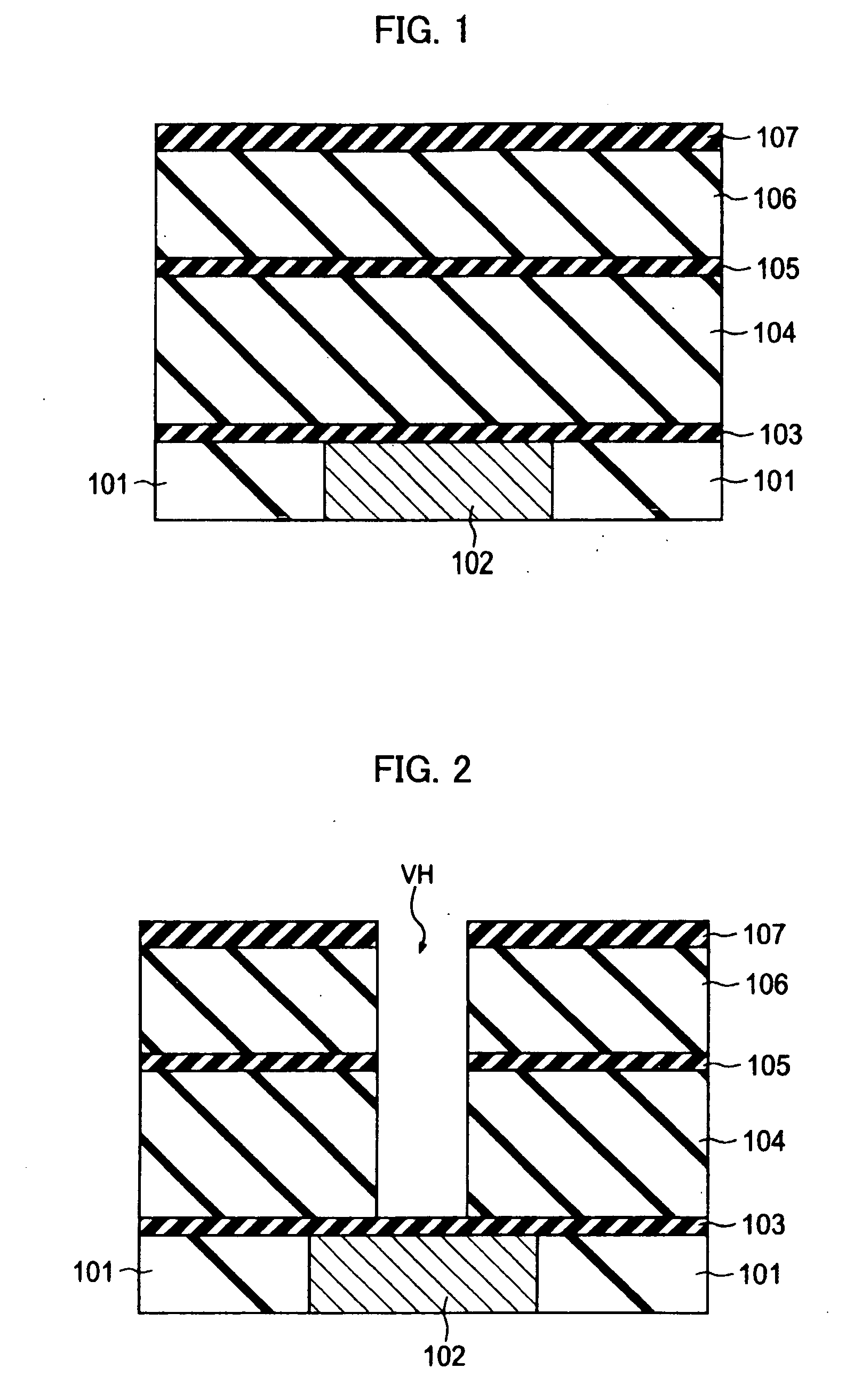
[0051] A conductive material is buried in a first interlayer insulation film 1 and a lower level wiring layer 2 is formed. On the first interlayer insulation film 1, an etching stopper film 3, a second interlayer insulation film 4, an etching stopper film 5, a third interlayer insulation film 6 and a hard mask film 7 are stacked in order.
[0052] A via hole is formed on the etching stopper film 3 and the second interlayer insulation film 4. The via hole has a pattern of an isolated approximately circular shape or a short trench shape when looking from the above, and is provided suitably on a required portion on the long lower level wiring layer 2.
[0053] A wiring trench ...
second embodiment
[0110] As a modified example of a first embodiment, the second interlayer insulation film 4 formed with a via hole can be composed of an inorganic based insulation material.
[0111] In the step shown in FIG. 10, instead of the second interlayer insulation film 4 composed of an organic based insulation material, a second interlayer insulation film composed of an inorganic based insulation material, for example, silicon oxide is formed. The inorganic based second interlayer insulation film will be referred to by the reference number 40 in the explanation below and in drawings.
[0112] A via hole VH is formed by switching from an organic based etching condition to an inorganic based etching condition in the same way as in FIG. 11, and silylation of the organic based interlayer insulation film and formation of a protective layer are performed in subsequent steps shown in FIG. 12 and FIG. 13.
[0113]FIG. 19 is a sectional view after the formation of a protective layer in the second embodime...
third embodiment
[0121] In the above first and second embodiments, when the organic based interlayer insulation films are composed of a porous film, diffusion of a silylating agent is accelerated and a silylated layer or a silylating agent diffusion layer can be easily formed.
[0122] A specific example of forming the porous film is as below.
[0123] As the third interlayer insulation film 6 (and second interlayer insulation film 4) shown in FIG. 10, a porous type polyarylether based resin is used. Since there are a number of vacancies, a silylating agent easily diffuses in the silylation step shown in FIG. 12, and a more stable silylating agent diffusion layer, silylated layer and silicon oxide film (protective layer) are formed on the hole inner walls.
[0124] An interlayer insulation film of a porous type polyarylether based resin is obtained by performing spin-coating of a liquid material obtained by dissolving a polyarylether based polymer and organic oligomer in a solvent on a substrate, spinning...
PUM
 Abstract
Description
Claims
Application Information